Semiconductor back-end manufacturing process
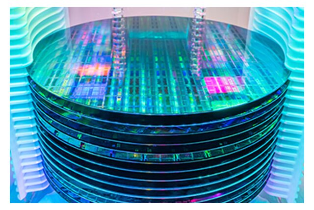
Back-end semiconductor manufacturing transforms processed wafers into functional, tested and traceable semiconductor devices. In this phase, wafers are thinned, separated, assembled, packaged and electrically validated. Each step adds value, but also introduces new risks if process conditions are not kept stable.
Unlike front-end processing, where structures are created at nanometer scale, back-end manufacturing is about handling fragile wafers and dies at high speed while maintaining micron-level precision, repeatability and cleanliness. Small deviations in transport, pressure, positioning or electrostatic conditions can directly affect yield, final package reliability and throughput.
That is why back-end equipment must be designed as an integrated process flow, not just as a sequence of isolated machines.
What defines stability in back-end semiconductor processes?
In back-end manufacturing, process stability means that devices, wafers and trays move through each step in a repeatable and controlled way, without introducing damage, contamination or misalignment.
This includes:
- accurate wafer and die positioning
- stable vacuum and pressure conditions
- controlled transfer into cutting, bonding and test operations
- electrostatic and contamination control
- reliable sorting and routing at the final stages
Instability introduced at one step often appears later, for example as die breakage during dicing, misplacement during die bonding or contact errors during test handling. Maintaining stable transfer and detection across the entire chain is therefore critical.
Why back-end processes must be viewed as one continuous flow
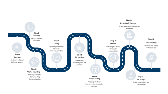
Back-end semiconductor manufacturing is not simply a collection of separate steps. It is a tightly linked process flow in which each stage prepares the wafer or device for the next one.
A typical flow includes:
- Probing – electrical verification before singulation
- Grinding – reducing wafer thickness
- Wafer mounting - Securing wafers for stable handling during singulation
- Dicing – separating the wafer into individual dies
- Die bonding – placing dies onto the package substrate
- Wire bonding – creating electrical interconnects
- Molding - Protecting the device with a stable encapsulation
- Trimming & Forming - Shaping leads for reliable board integration
- Marking – ensuring traceability
- Test handling – routing, contacting and sorting finished devices
The exact order can vary depending on device architecture and package type, but the principle remains the same: stable handling and precise detection are required at every step.
Probing - Verifying electrical functionality before singulation
Probing tests the electrical behaviour of dies while they are still on the wafer. Only known-good dies move forward into subsequent assembly and packaging steps.
At this stage, accuracy in positioning and contact is essential. Reliable probing ensures that only functional devices continue through the back-end process, reducing downstream waste and improving overall line efficiency.
Impact: establishes the electrical baseline before further processing
Grinding - Defining wafer thickness for advanced packaging
Grinding reduces wafer thickness to support compact packages, thermal performance and miniaturized device architectures. As wafers become thinner, they also become more fragile, making stable vacuum fixation and pressure control essential.
Reliable grinding depends on precise wafer adsorption, accurate positioning, stable cooling and monitoring of wear conditions.
Impact: defines wafer thickness and mechanical readiness for singulation
Wafer mounting - Securing wafers for stable handling during singulation
Before dicing, wafers are mounted onto a carrier film to ensure stable handling. Correct alignment and secure fixation are essential to prevent stress or misalignment in later steps.
Impact: creates a stable starting point for cutting and handling
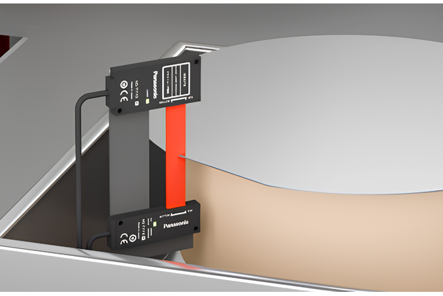
Dicing - Separating wafers into individual dies with minimal damage
Dicing cuts the wafer into separate dies using saw or laser-based systems. At this stage, even small positioning errors, unstable suction or insufficient cooling can lead to chipping, contamination or die loss.
Stable dicing requires precise wafer fixation, protrusion detection, blade monitoring and continuous cooling control.
Impact: determines die integrity and yield before assembly
.
Die bonding - Placing each die accurately onto the package substrate
Die bonding attaches the singulated die to the package or substrate. This step must be performed with high positional accuracy to ensure both mechanical stability and downstream interconnection quality.
Reliable die bonding depends on accurate die detection, controlled pick-and-place movement and stable contact conditions throughout the transfer.
Impact: defines die placement accuracy in the final package
Wire bonding - Creating reliable electrical interconnections
Wire bonding connects the die to the package using ultra-thin conductive wires. This step is essential for enabling current and signal flow between the semiconductor die and the package leads.
Because wire bonding requires micron-level precision, stable positioning and process consistency are critical to ensure long-term electrical reliability.
Impact: establishes electrical continuity inside the final package
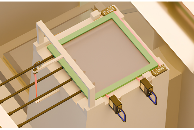
Molding - Protecting the device with a stable encapsulation
Molding encapsulates the die and wires in a protective resin, shielding them from environmental influences such as moisture, dust and mechanical stress.
Impact: protects the device and ensures long-term reliability
Trimming & Forming - Shaping leads for reliable board integration
In this step, excess material is removed and leads are shaped to their final geometry. Accurate handling and positioning ensure uniform lead structure and reliable mounting on PCBs.
Impact: defines mechanical fit and connectivity
Marking - Ensuring traceability and identification
Marking adds codes, identifiers or logos to the package surface. Although it is often seen as a finishing step, its reliability is critical for downstream traceability, quality control and logistics.
Stable positioning and repeatable operation are essential to ensure that every device is marked accurately and consistently.
Impact: enables identification and full product traceability
Test handling - Routing devices reliably through final validation
Test handling moves packaged devices into electrical contact, through sorting and into the correct bin after test. At this stage, transfer speed is high, but positioning must remain highly accurate to avoid contact errors, misfeeds or incorrect binning.
Reliable device presence detection, vacuum control, static elimination and routing verification are essential to maintain final output quality.
Impact: confirms final quality and ensures correct device binning
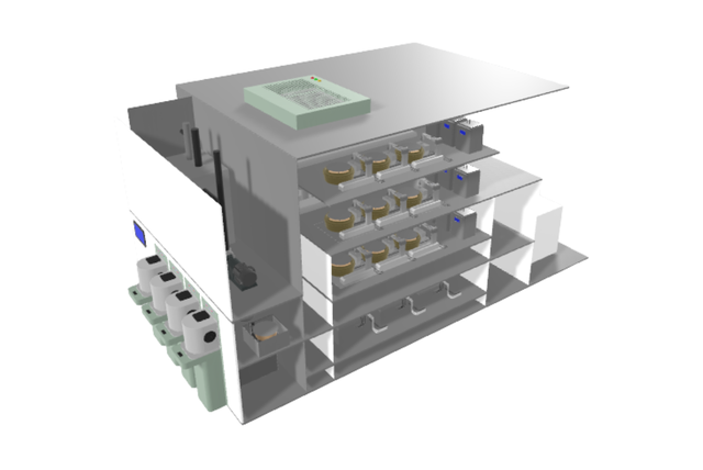
Why system-level stability matters in back-end manufacturing
Back-end manufacturing is where design intent becomes a shippable product. The main risks at this stage are no longer only process-physics related, but also mechanical and logistical: handling fragile materials, maintaining alignment at speed and ensuring every die and device moves through the correct route.
This is why success in back-end equipment depends on more than one sensor or one machine. It depends on whether the entire process flow remains stable, repeatable and controllable as one system.
Panasonic Industry supports this system-level approach with sensing, ionization, pressure, leakage and safety technologies designed for compact, high-speed and contamination-sensitive semiconductor equipment.
Panasonic Industry solutions for back-end semiconductor equipment
Panasonic Industry supports semiconductor equipment builders with:
- compact sensing for space-constrained systems
- pressure and vacuum monitoring for reliable handling
- fiber-optic and photoelectric detection for high-precision transport
- ionizers for electrostatic control
- leakage and process monitoring for uptime and safety
These technologies help ensure that back-end processes remain stable from wafer to finished device, supporting both engineering performance and production scalability.