

Semiconductor back-end probing process
In semiconductor back-end manufacturing, probing is the first critical electrical test step before wafers are diced and packaged. During wafer probing, each die is electrically contacted and tested while still on the wafer, allowing defective dies to be identified before they move further into assembly and packaging.
This early validation step is essential because packaging defective dies creates unnecessary downstream cost, complexity and material waste. Probing therefore acts as a quality gate between wafer fabrication and back-end assembly.
At this stage, stable wafer positioning, accurate contact, controlled pressure and clean handling conditions all matter. Even small deviations in alignment, suction, temperature or electrostatic charge can influence test accuracy or damage sensitive pads.
What challenges define the probing process?
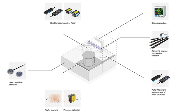
Wafer probing combines precision mechanics, electrical contact and automated handling. The wafer must be positioned accurately under the probe card, while the probe needles or contact elements must make reliable electrical contact with the die pads or bumps.
As pad sizes shrink, pin counts increase and device architectures become more complex, the process becomes more sensitive to alignment errors, contact force instability and wafer movement. Advanced probing often requires micron-level coordinate control and compensation for effects such as wafer warpage, thermal drift or die shift.
For equipment builders, this means that probing is not only about electrical test. It is about maintaining stable mechanical and environmental conditions so that test data reflects the die performance, not instability in the test setup.
Wafer positioning and alignment
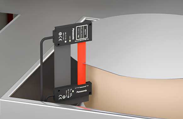
Ensuring accurate contact between probe card and die pads
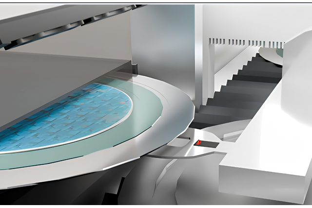
Accurate wafer positioning is fundamental in probing. The probe card must align with the correct pads or bumps on each die, and even small positioning errors can lead to poor contact, false failures or pad damage.
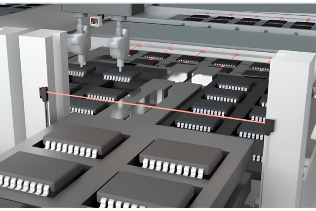
Panasonic Industry supports this process with HG‑T laser thru-beam displacement sensors and HL‑G2 laser displacement sensors. The HG‑T series uses a belt-shaped laser beam and provides high-precision, stable measurement for position and contour detection, while the HL‑G2 series offers high-speed, high-accuracy displacement measurement with digital communication options.
By monitoring wafer or stage positioning with stable displacement feedback, these sensors help maintain repeatable alignment and reduce the risk of contact-related test variation.
Chuck vacuum and wafer fixation
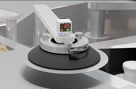
Keeping the wafer stable during electrical testing
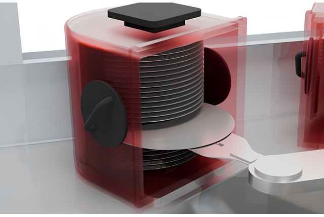
During probing, the wafer is held on a chuck, often using vacuum fixation. Stable wafer fixation is important because movement during contact can affect measurement reliability and may lead to inconsistent probe force or pad stress.
Panasonic Industry supports suction and pressure monitoring with DP‑100 digital pressure sensors. The DP‑100 series provides high-resolution pressure sensing with a dual three-colour display, allowing current values and threshold values to be checked simultaneously.
By monitoring vacuum and pressure conditions, equipment builders can verify wafer fixation before testing begins and detect instability before it affects probing accuracy.
Contact stability and process repeatability
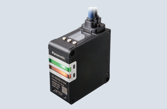
Preventing false failures during wafer-level testing
Wafer probing is used to classify dies based on electrical performance. If the mechanical contact is unstable, the test result may reflect contact variation rather than actual die quality. This can lead to false failures, retest cycles or misclassification.
Stable positioning feedback from HG‑T and HL‑G2 sensors can support repeatable contact conditions by verifying critical motion, position and distance parameters in the prober system. The HL‑G2 series is designed for high-precision measurement, with high-speed sampling and integrated communication options that support digital data acquisition and monitoring.
This helps improve test consistency and supports more reliable wafer maps for downstream dicing and assembly.
Electrostatic charge control
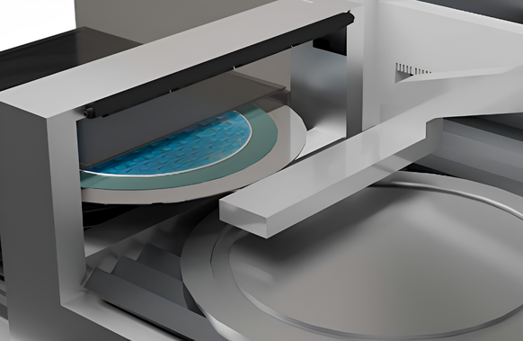
Protecting sensitive dies and reducing particle attraction
During wafer handling and test operations, electrostatic charge can attract particles or create risks for sensitive semiconductor structures. In clean and high-precision environments, charge control helps maintain stable handling and reduces contamination risk.
Panasonic Industry supports electrostatic control with the ER‑X ionizer, designed for wide-area charge removal with or without compressed air. The ER‑X series supports different charge removal modes, including airless and low-pressure operation, which is relevant for applications requiring cleanliness and minimal dust dispersion.
By neutralising charge around wafer handling and test areas, ionization supports cleaner and more predictable probing conditions.
Leak detection and system safety
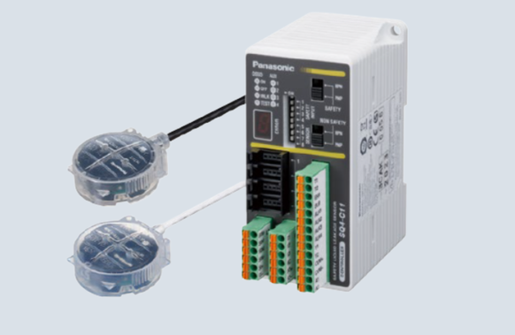
Protecting uptime in probe equipment
Probe equipment may include cooling and environmental control systems that must remain stable during operation. Leakage or abnormal liquid conditions can create downtime, safety risks or contamination issues.
Panasonic Industry supports this with the SQ4 safety liquid leak sensor, which provides two-stage detection for early leak warning and emergency stop. The SQ4 is designed to support safety concepts such as Type 4, PLe and SIL3 when used in the appropriate configuration.
This allows equipment builders to monitor leak risks while balancing uptime and safety.
Why probing stability matters for downstream performance
Probing determines which dies continue into dicing, bonding, packaging and final test. If probing is unstable, functional dies may be rejected unnecessarily, or marginal issues may be missed.
Reliable probing supports:
- better known-good-die selection
- reduced downstream processing of defective dies
- improved yield feedback to wafer fabrication
- more predictable back-end flow
Because test data is used for decisions later in the process, probing must be stable, repeatable and traceable.
Panasonic Industry solutions for probing processes
Panasonic Industry supports semiconductor probing equipment with sensing, pressure monitoring, ionization and safety technologies designed for precise and stable automation.
These include:
- HG‑T laser thru-beam displacement sensors for stable measurement
- HL‑G2 laser displacement sensors for high-accuracy positioning
- DP‑100 pressure sensors for vacuum monitoring
- ER‑X ionizers for electrostatic control
- SQ4 leak sensors for safety-related liquid leak detection.
Together, these technologies help equipment builders maintain stable wafer test conditions and support reliable back-end manufacturing.
FAQ – Wafer Probing
|
Why is wafer probing important in semiconductor manufacturing? |
Wafer probing is important because it verifies the electrical performance of each die before dicing and packaging. This allows defective dies to be identified early, reducing unnecessary downstream processing and improving yield efficiency. |
|
What makes wafer probing challenging? |
Wafer probing is challenging because it requires precise alignment between the probe card and the die pads or bumps. As devices become more complex and pad pitches become smaller, even small alignment errors can cause poor contact, false failures or pad damage. |
|
How does wafer positioning affect probing accuracy? |
Wafer positioning determines whether the probe card contacts the correct locations on each die. If the wafer or stage is not positioned accurately, the electrical test may become unreliable or may damage sensitive contact pads |
|
Why is chuck vacuum important in wafer probing? |
Chuck vacuum keeps the wafer stable during probing. If the wafer moves during contact, contact force and measurement reliability may be affected. Pressure monitoring helps verify that the wafer is securely fixed before and during testing. |
|
How does electrostatic control support wafer probing? |
Electrostatic control helps reduce particle attraction and protects sensitive wafer structures during handling and test operations. Ionizers can neutralise charge around the wafer handling area, supporting cleaner and more predictable test conditions. |