Laser Marking Solutions for the Semiconductor Industry
In the fast-evolving world of semiconductor manufacturing, precision and traceability are critical. At Panasonic Industry, we offer cutting-edge laser marking solutions tailored to meet the unique challenges of the semiconductor industry, where speed, miniaturization, and product identification are paramount. Our systems ensure seamless integration into your production lines, offering precision, speed, and environmental benefits that keep your operations efficient and sustainable.
Why Laser Marking?
The semiconductor industry demands robust, non-contact solutions for identifying components, and laser marking is ideally suited for this environment. Our systems deliver:
- Non-contact marking that avoids damage to delicate components.
- Permanent and precise markings to ensure traceability and compliance.
- High-speed marking for fast-moving production lines.
- Environmentally friendly technology with no waste materials or consumables.
By integrating laser marking into your production processes, you can ensure compliance, reduce downtime, and enhance quality control in a cost-effective and sustainable way.
Our Laser Marking Systems
Explore the Panasonic Industry laser marking systems designed specifically for the semicon industry:
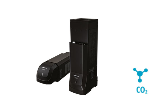
LP-RH CO2 Laser Technology
Explore the Panasonic Industry laser marking systems designed specifically for the semicon industry:
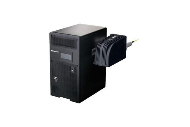
LP-RH CO2 Laser Technology (plus picture of this laser)
Ideal for high-speed production environments, the LP-RH series leverages CO2 laser technology to deliver up to 240 markings per minute, all while maintaining exceptional precision. This system is perfect for high-throughput semiconductor processes where speed is of the essence. Its on-the-fly marking capabilities make it an excellent choice for dynamic back-end semiconductor production.
LP-ZV 3D Fiber Laser Technology
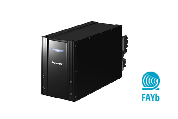
For more complex workpieces with varying heights, the LP-ZV series offers 3D fiber laser technology with an ultra-short pulse duration of 1 nanosecond. It can handle slanted, convex, and concave surfaces with ease, thanks to its integrated Z-axis control. This makes it the go-to solution for precision marking on intricate components such as sensors, diodes, and IC housings.
Customized Solutions for Your Semiconductor Needs
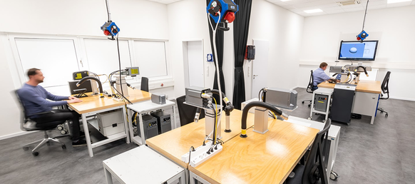
At Panasonic Industry, we understand that every production environment is unique. That’s why we offer customized laser marking solutions. From feasibility studies to custom-built workstations, we work closely with our clients to provide solutions that fit their specific needs. Our support extends beyond installation, offering training and maintenance to ensure your system continues to operate at peak performance.
Need expert advice on which solution fits your production line best? Contact us today for personalized assistance.
Supporting Your Semiconductor Operations Globally
With Panasonic Industry’s global support network, including our expert team based in Best, the Netherlands, you can rely on us for fast, responsive service. Our extensive experience in the semicon industry, combined with the backing of our international parent company, ensures that we’re always here to help you succeed.
