Front-End semiconductor manufacturing: precision sensing and control
Front‑end semiconductor manufacturing consists of tightly coupled process steps where stability directly determines yield, repeatability and scalability.
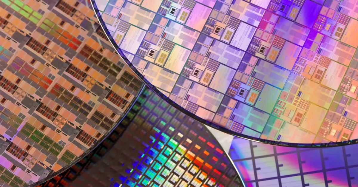
Processes such as cleaning, exposure, developing and etching operate at nanometer scale. At this level, even small variations in:
- wafer positioning
- contamination control
- electrostatic charge
- or process timing
can propagate through the entire process chain and result in yield loss.
This is why semiconductor equipment builders must design systems that ensure stable behavior across all front‑end process steps, not just within individual modules.
What defines stability in front end semiconductor processes?
In semiconductor manufacturing, process stability means:
- repeatable wafer handling across all process steps
- controlled contamination and particle behavior
- predictable process results from wafer to wafer
- consistent performance during High‑Volume Manufacturing (HVM)
Instability in one process step often becomes visible in later stages, making early detection and control critical.
What semiconductor equipment requires from sensing and control

To achieve stable front‑end processing, equipment builders need technologies that are:
- Compact
to fit into space‑constrained tool architectures - Stable
to ensure repeatable detection and motion control - Non‑intrusive
to avoid interference with sensitive processes such as lithography - Reliable over time
to support lifecycle stability and reduce requalification risk
Panasonic Industry solutions for front end semiconductor equipment
Panasonic Industry provides sensing, ionization, automation and safety technologies designed for semiconductor environments, supporting:
- wafer detection and positioning
- electrostatic charge control
- contamination‑resistant sensing
- leak detection and process safety
- compact integration in advanced equipment
These technologies are used across multiple front‑end steps and help ensure system‑level stability, from prototyping to HVM and global fab deployment.
Cleaning - Preparing the wafer surface for subsequent processes
Cleaning removes particles and chemical residues from the wafer surface before patterning begins. Even microscopic contamination can disrupt nanoscale structures and affect all downstream processes.
A clean and stable surface is essential to ensure that subsequent layers adhere correctly and that processing conditions remain predictable.
Impact: establishes the foundation for yield and process stability
Film Deposition - Building uniform thin films as the foundation for device structures

During deposition, ultra‑thin layers such as oxides or nitrides are added to the wafer. These films define electrical properties and form the basis for later processing.
Stable wafer positioning, controlled environmental conditions and non‑intrusive sensing are essential to ensure uniform layer growth.
Impact: defines layer uniformity and electrical performance
Resist Coating - Applying a uniform photoresist layer for pattern definition
Resist coating applies a photosensitive layer onto the wafer, which will later be patterned during lithography. Uniform coating thickness and stable conditions are critical to ensure accurate exposure results.
Variations in liquid dispensing, wafer alignment or electrostatic conditions can introduce deviations that only become visible in later steps.
Impact: determines coating uniformity and lithography accuracy
Exposing (Lithography) - Transferring patterns with nanometer precision
During exposure, patterns are projected onto the photoresist layer, defining critical dimensions and overlay accuracy. This is one of the most sensitive steps in the process.
Even small deviations in wafer or reticle positioning directly affect pattern fidelity and ultimately device performance.
Impact: defines the final circuit structure
Developing - Revealing the pattern for subsequent processing
In the developing step, exposed photoresist is selectively removed to create a stable pattern. This step translates lithography into a physical structure that can be transferred into the wafer.
Process stability here is essential, as variations in liquid delivery or wafer handling can influence pattern reproducibility.
Impact: determines pattern consistency and reproducibility
Etching - Transferring patterns into material layers
Etching removes material selectively using plasma or chemical processes to transfer the developed pattern into underlying layers. This step defines the physical structure of the device.
Precise control of wafer positioning, detection and process conditions is required to maintain pattern fidelity.
Impact: creates final structures and layer definition
Ion Implantation - Defining electrical properties at atomic level
Ion implantation introduces dopants into the wafer at controlled depth, defining electrical conductivity and device behaviour. This process requires precise beam control and accurate wafer positioning.
Instability at this stage directly affects device performance and cannot easily be corrected later.
Impact: determines electrical characteristics of the device
Resist Stripping - Restoring a clean wafer surface for the next cycle
After etching, the remaining photoresist must be removed completely to prepare the wafer for subsequent processing steps. Plasma and wet cleaning processes remove residues and particles.
Stable process control and monitoring are essential to ensure complete removal without damaging the wafer surface.
Impact: resets surface conditions for next process cycle
Why system-level stability matters
Each of these steps is part of a continuous process flow. Instability introduced at one stage will often only become visible later, making root cause analysis complex and costly.
For semiconductor equipment builders, this means that success is not defined by individual components, but by how well all process steps are aligned and controlled as one system.
Panasonic Industry supports this approach with sensing, control and automation technologies designed to ensure stability across the entire front-end manufacturing chain.