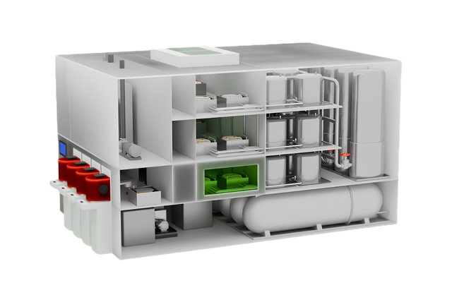
Semiconductor front end developing process
In semiconductor front‑end manufacturing, the developing step transforms the exposed photoresist into a usable pattern for subsequent processing.
After lithographic exposure, the wafer enters the development stage where the exposed or unexposed resist is selectively dissolved, depending on the process type. The quality and stability of this step directly determine how accurately the final pattern can be transferred during etching.
At nanometer scale, even small variations in development conditions can result in:
- inconsistent pattern dimensions
- edge roughness
- local defects
- downstream etch variation
For semiconductor equipment builders, this makes stable wafer handling, liquid control and process monitoring essential during development.
What challenges define the developing process?
The developing step must ensure that:
- resist removal is uniform across the wafer
- flow conditions are stable and repeatable
- no contamination or bubbles disturb local chemistry behavior
- wafers are handled without introducing mechanical or electrostatic variation
Typical challenges include:
- instability in liquid delivery
- air bubbles in chemistry lines
- incorrect wafer positioning
- electrostatic effects during handling
- contamination affecting resist interaction
The following sections describe how each challenge is addressed within the developing process.
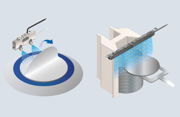
Liquid delivery and chemistry control
Ensuring stable resist development conditions
The development process depends on precisely controlled liquid delivery. Any variation in flow or composition directly influences resist dissolution behavior.
Key risks
- air bubbles disrupting local chemistry interaction
- inconsistent flow conditions
- contamination or particle presence in liquids
Panasonic solutions for liquid control
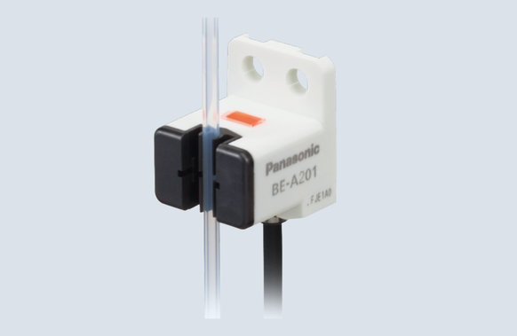
- Optical bubble sensors (BE‑A series)
Enable inline detection of air bubbles in small‑diameter tubes before chemistry reaches the wafer.
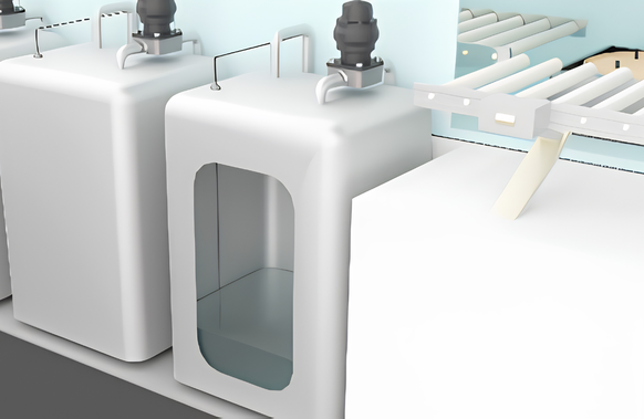
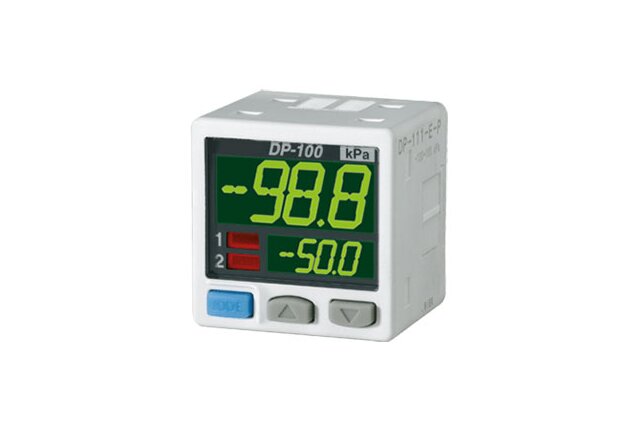
- Liquid level sensors (FD-HF series)
Provide stable, non‑invasive monitoring of liquid levels in tanks and supply systems.
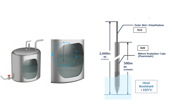
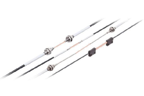
- Flow / process condition sensing (fiber-based solutions)
Allow detection in chemically aggressive environments without direct exposure of electronic components.
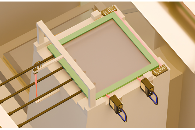
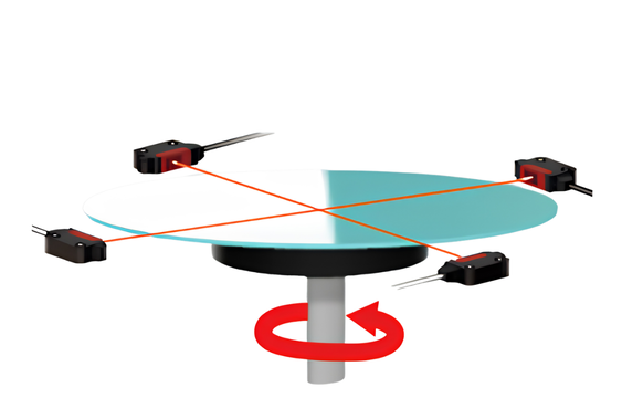
Wafer and reticle alignment
Ensuring positional accuracy before exposure
Accurate wafer and reticle alignment is essential to achieve overlay accuracy and pattern fidelity during lithographic exposure.
Key risks
- misalignment during wafer centering
- positional drift caused by vibration or temperature variation
- limited installation space near alignment stages
Panasonic solutions for Alignment
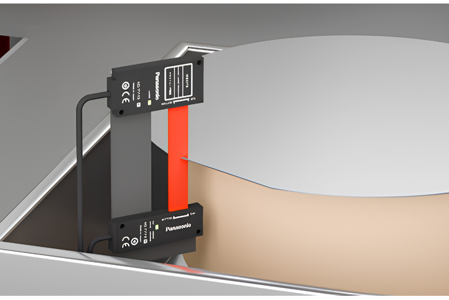
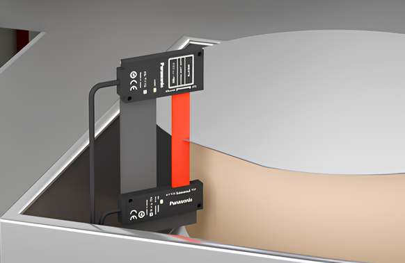
- HG‑T digital displacement sensors
Enable precise notch and eccentricity detection for wafer centering with micrometer‑level repeatability.
- HL‑G2 laser displacement sensors
Provide high‑speed feedback for alignment control on reflective surfaces in lithography environments.
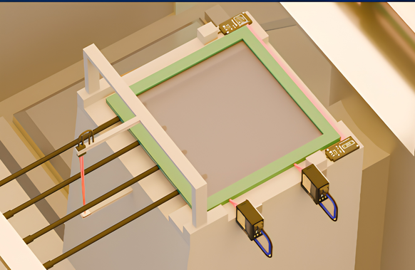
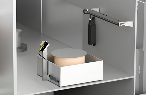
Wafer presence, positioning and handling
Preventing variation during processing
During development, correct wafer positioning ensures uniform interaction between the resist and the process chemistry.
Key risks
- wafer misalignment leading to uneven development
- incorrect wafer seating on robot blades or process stages
- wafer tilt or protrusion during transfer
- undetected missing or double wafer presence
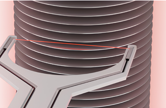
Panasonic solutions for wafer handling
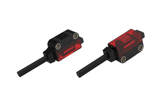
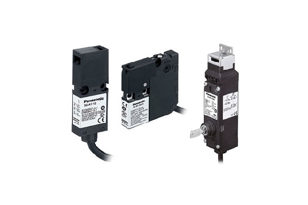
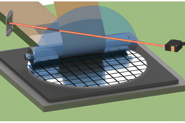
- Chemical‑resistant fiber sensors (FT series)
Enable reliable wafer presence detection in wet and chemically aggressive environments.
- Compact laser sensors (EX‑L200)
Provide stable positioning and alignment detection, even through protective covers or in constrained spaces.
- Narrow‑beam fiber sensors (FT‑KV series)
Support precise wafer detection on robot arms, enabling accurate wafer mapping, centering and correct pick‑and‑place verification.
Electrostatic charge control
Preventing particle attraction and resist disturbance
Electrostatic charge can influence particle behavior and resist interaction, especially in dry‑to‑wet transitions.
Key risks
- particle attraction affecting resist quality
- wafer sticking or unstable handling
- unpredictable surface interactions
Panasonic solutions for static control
- ER‑X and ER‑V ionizers
Neutralize electrostatic charge during wafer transfer and processing.
- EF‑S1 surface potential sensors
Provide insights into residual charge levels for process optimization.
Leak detection and safety monitoring
Ensuring uptime and process reliability
Developing equipment relies on fluid systems that must be continuously monitored.
Key risks
- leaks in chemical delivery systems
- unexpected downtime
- safety hazards
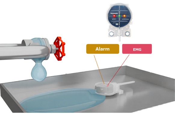
Panasonic solutions for safety and monitoring
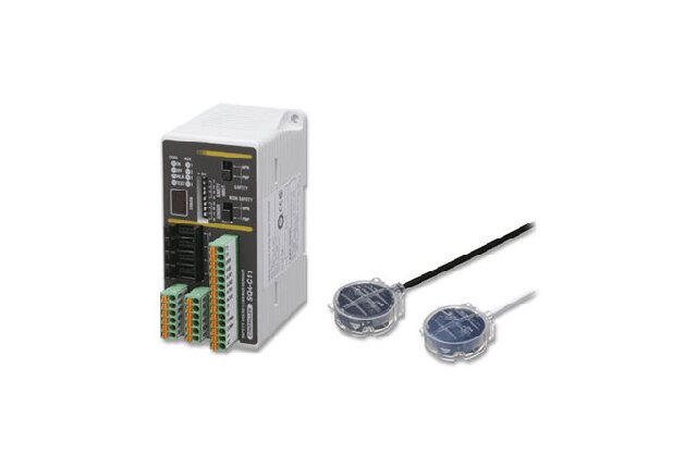
- SQ4 leakage sensors
Provide reliable detection with early warning and emergency stop capability.
Why stability during developing matters for downstream processes
The developing step directly influences pattern accuracy before etching, line edge quality, repeatability across wafers and yield in later process stages.
Instabilities during developing are often not visible immediately, but appear later as:
- etch deviations
- yield loss
- increased metrology corrections
This makes developing a critical control point for overall front‑end process stability.
Panasonic Industry solutions for developing processes
Panasonic Industry supports semiconductor equipment builders with:
- chemical‑resistant sensing solutions
- compact designs for space‑constrained wet processing tools
- stable detection independent of contamination and bubbles
- integrated solutions for handling, liquid control and safety
These technologies enable repeatable, stable and scalable developing processes, supporting both prototyping and HVM environments.