Process stability starts before measurement and patterning
Front‑end cleaning is one of the most contamination‑sensitive stages in the semiconductor process. Any residual particle, chemical droplet or electrostatic charge can impact adhesion, layer uniformity and ultimately device yield.
Modern cleaning equipment must handle:
- aggressive chemicals (acids, solvents, DI water, IPA)
- ultra‑thin and fragile wafers
- tight process windows
- high uptime requirements
This makes reliable sensing, liquid control and static management essential throughout the entire cleaning process.
Panasonic Industry supports semiconductor cleaning equipment with sensors, fibers, laser solutions, ionizers and safety devices designed specifically for chemical, wet and space‑critical environments.
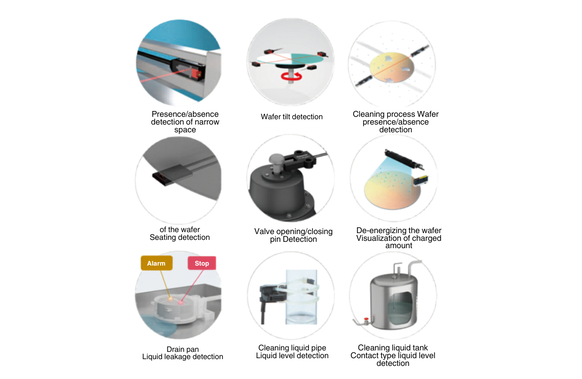
Typical challenges in front end cleaning equipment
In real tools, cleaning issues rarely come from one source. Common challenges include:
- unstable liquid supply or unnoticed leaks
- air bubbles in chemical lines
- wafer misalignment, tilting or improper seating
- electrostatic charge during transfer and drying
- sensor degradation due to chemicals, heat or contamination
The following sections break down the cleaning process step‑by‑step and show how these challenges are addressed.
Chemical supply & liquid management
Stable chemistry delivery without leaks, bubbles or level errors
In semiconductor cleaning, contamination is rarely introduced in one moment, but typically through small instabilities in liquid delivery and wafer handling.
Key risks
- unnoticed leaks in drain pans or piping
- air bubbles disturbing dosing consistency
- incorrect liquid levels in tanks
- sensor failure due to heat or chemicals
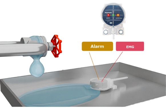
Liquid leakage detection
SQ4 safety leakage sensor
- two‑stage detection: early leakage alarm + emergency stop
- supports SEMI S2, PLe / SIL3
- chemical‑resistant and reliable in real fab conditions
Bubble detection in chemical lines
BE‑A optical bubble sensors
- inline detection for small‑diameter tubing
- detects bubbles without flow obstruction
- prevents bubbles reaching the wafer
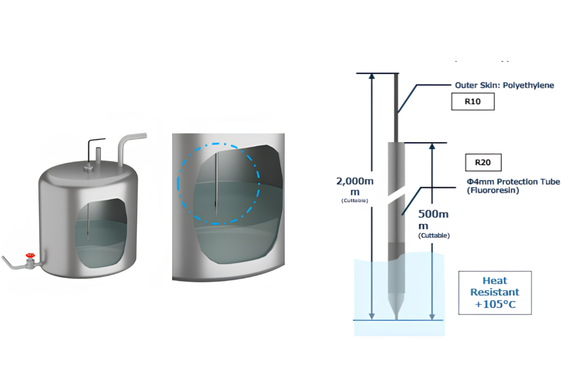
Liquid level detection
FD‑HF / FD‑F series fiber heads
- metal‑less, chemically resistant
- IP68G protection
- stable detection regardless of bubbles or deposits
Result: stable dosing, reduced downtime and higher process repeatability.
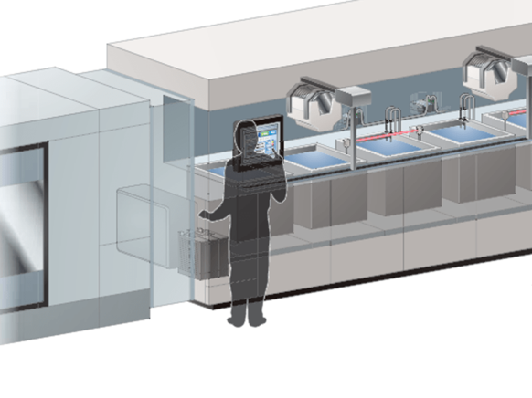
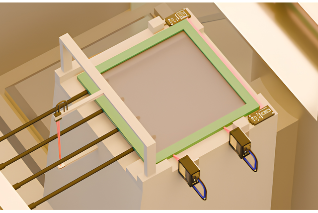
Wafer presence, seating & tilt detection
Prevent mechanical damage and contamination at wafer level
During cleaning, wafers are extremely vulnerable. Even small positioning errors can cause breakage or particles.
Key risks
- wafer tilt inside the cleaning chamber
- incorrect seating on pins or robot blades
- wafer protrusion causing contact or chipping
Wafer presence & seating
Chemical‑resistant fibers
- metal‑less construction
- compatible with aggressive chemicals
- stable detection in wet environments
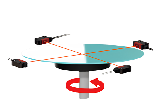
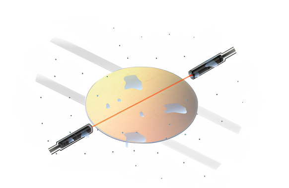
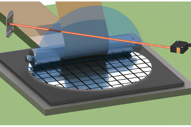
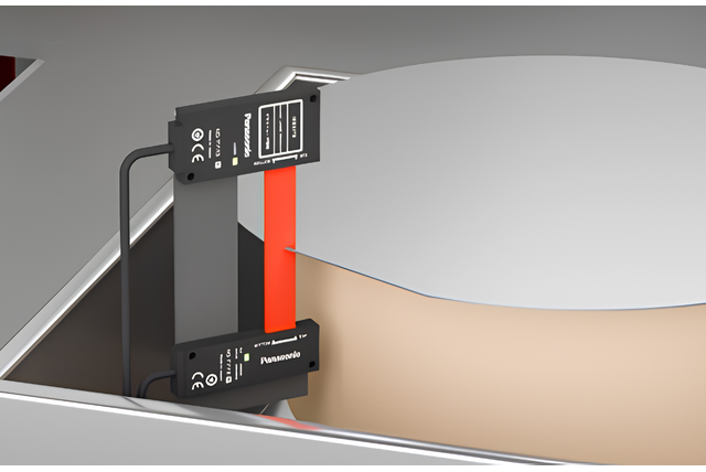
Wafer tilt and alignment
EX‑L200 ultra‑compact laser sensors
- built‑in amplifier
- stable through viewports
- Class 1 laser for safe use near operators
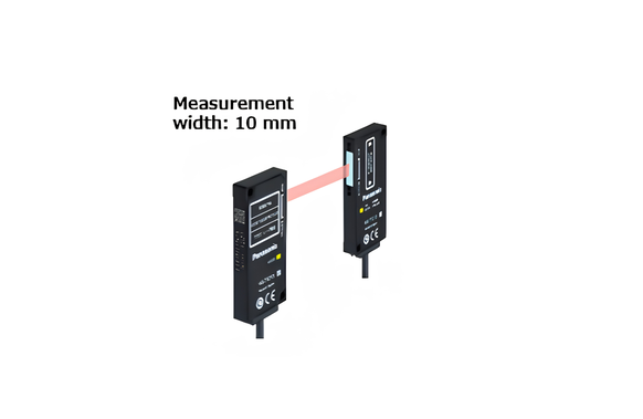
Fine positioning & mechanical monitoring
HG‑C CMOS laser sensors
HG‑T digital displacement sensors
- micrometer‑level repeatability
- analog, IO‑Link or network connectivity
Result: reduced wafer breakage, higher yield and safer operation.
Static control during cleaning & drying
Eliminate charge before it becomes contamination
Electrostatic charge is often underestimated in cleaning processes, especially during transfer, spin drying or IPA drying.
Key risks
- particle attraction due to electrostatic charge
- wafer sticking or unpredictable movement
- ESD‑related yield loss
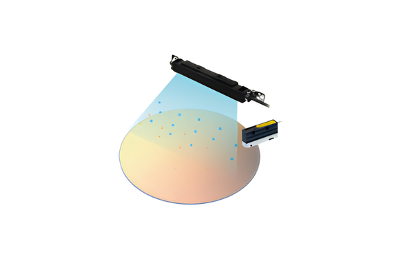
Ionization
- ER‑X pulsed AC area ionizers
- ER‑V compact ionizers
Charge visualization
EF‑S1 surface potential sensors
- visualize residual charge
- enable controlled discharge strategies
Result: cleaner wafers, more predictable handling and lower contamination risk.
Sensors designed for chemical & harsh environments
Cleaning tools demand sensors that survive where standard devices fail.
Panasonic technologies are designed with:
- metal‑less fiber heads for chemical resistance
- heat resistance up to 100 °C–150 °C (and higher where required)
- slim designs for integration in narrow tool layouts
- amplifier separation to keep electronics away from aggressive environments
This makes them suitable for:
- wet benches
- spray and immersion cleaning
- IPA drying
- confined chambers
FAQ's Front‑end cleaning process
|
Why is front‑end cleaning so critical in semiconductor manufacturing? |
Because even microscopic contamination introduced during cleaning can compromise adhesion, patterning accuracy and overall device yield in later process steps. |
|
What are the most common causes of instability in cleaning equipment? |
Typical causes include unnoticed liquid leaks, air bubbles in chemical lines, wafer misalignment, electrostatic charge during drying and sensor degradation due to chemicals. |
|
Why are chemical‑resistant and metal‑less sensors important in cleaning tools? |
Metal‑less and chemically resistant sensor heads prevent corrosion, particle generation and false detection in aggressive wet and chemical environments. |
|
How does bubble detection improve cleaning consistency? |
Air bubbles disrupt liquid continuity and dosing accuracy. Inline bubble detection prevents disturbances from reaching the wafer before they impact the process. |
|
Why use two‑stage leakage detection instead of a single alarm? |
Two‑stage detection allows minor leaks to be addressed without stopping the tool, while still triggering an emergency stop when a safety‑critical threshold is reached. |
|
How does static electricity affect cleaned wafers? |
Electrostatic charge attracts particles, causes sticking effects and can lead to unpredictable wafer movement during drying or transfer. |
|
Are Panasonic cleaning solutions suitable for space‑constrained equipment? |
Yes. Many Panasonic sensors, fibers and safety devices are designed with ultra‑slim housings and separated amplifiers for integration in narrow tool layouts. |
|
Do these solutions support semiconductor safety standards? |
Yes. Selected products support SEMI S2 and functional safety levels up to PLe / SIL3, depending on system configuration. |