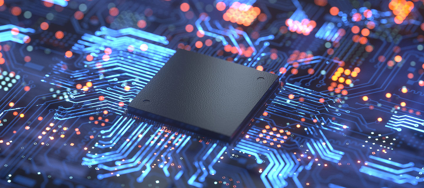
Semiconductor front-end etching process
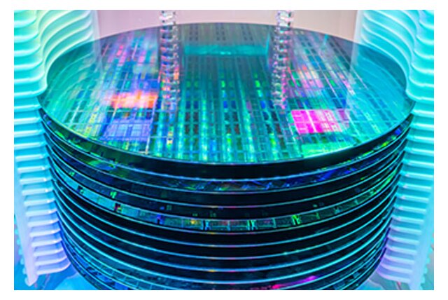
In semiconductor front-end manufacturing, the etching process translates lithographic patterns into physical structures by selectively removing material. Whether using dry plasma-based etching or wet chemical processes, this step directly determines how accurately patterns are transferred into the wafer.
At today’s feature sizes, even small variations in process conditions can impact etch profiles, uniformity and ultimately yield. That makes etching not just a material removal step, but a critical point where process stability, wafer handling and sensing all come together.
For semiconductor equipment builders, ensuring consistent behavior inside highly controlled environments is key to delivering repeatable results at scale.
What challenges define the etching process?
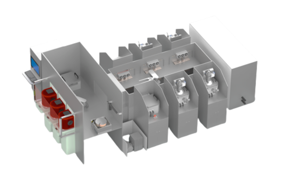
Etching processes operate in highly demanding environments, where conditions such as vacuum chambers, plasma-based dry etching and aggressive chemical media in wet processes all place strict requirements on equipment performance.
Within these environments, maintaining stability is not straightforward. Challenges arise around accurate wafer positioning and alignment inside the chamber, while detection often has to take place indirectly, for example through viewports. At the same time, electrostatic charge can build up and influence wafer behavior, and chemical processes introduce additional risks related to leakage and safety. All of this creates a complex interaction between sensing technologies and process conditions, making reliable detection and control a critical factor in overall process stability.
The following sections explain how these challenges can be addressed.
.
Wafer positioning and alignment in the chamber
Ensuring accuracy during etching and ion implantation
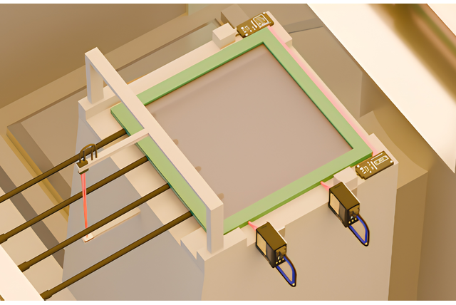
During the etching process, wafers must be positioned precisely to ensure uniform exposure to plasma or chemical media. Even slight misalignment can affect how material is removed, leading to variation in feature dimensions.
This level of precision is not trivial to maintain. Mechanical tolerances, thermal effects and movement during wafer placement all introduce variability. Because these deviations are often small, they are easy to overlook but can have a significant impact on final device performance.
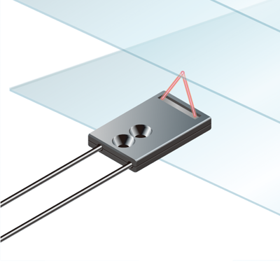
By integrating high-precision displacement sensors and compact laser technologies, it becomes possible to continuously verify positioning and alignment. This improves control over the process and helps maintain consistent etch results across wafers.
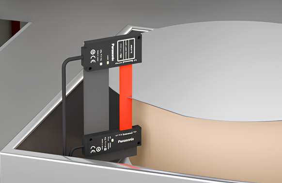
Panasonic Solutions
- Digital displacement sensors (HG‑T series)
Enable high-precision alignment and positioning detection, even in space‑constrained environments.
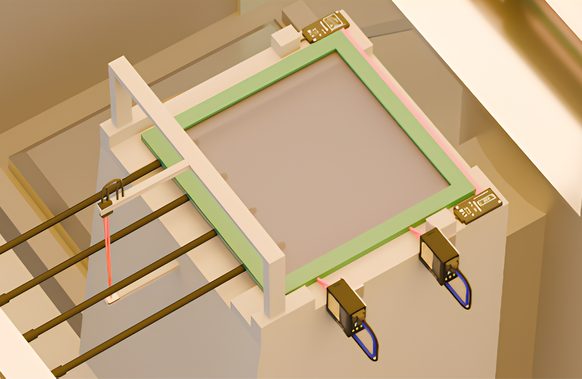
- Laser displacement sensors (HL‑G2 series)
Provide stable, high-speed measurement with micrometer-level repeatability for positioning critical components.
Detection through viewports and confined environments
Monitoring wafer position without disturbing the process
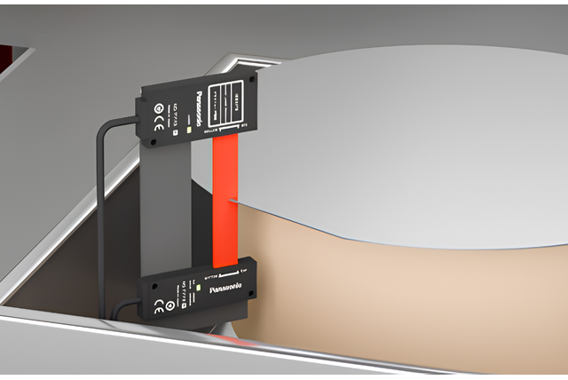
In many etching systems, wafers are processed inside sealed chambers, making direct sensing difficult. Detection must therefore take place from outside the process area, often through viewports.
This introduces challenges such as limited visibility, reflections and the need to avoid interference with vacuum or plasma conditions. Traditional sensing approaches can struggle in these environments.
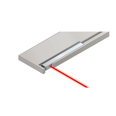
Laser-based sensing technologies with high directionality provide a solution by enabling accurate detection over distance. This makes it possible to monitor wafer position and movement without influencing the process itself, ensuring stable observation while maintaining the integrity of the etching environment.
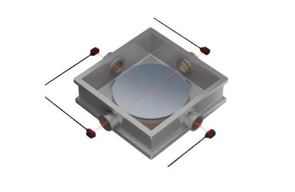
Panasonic solutions
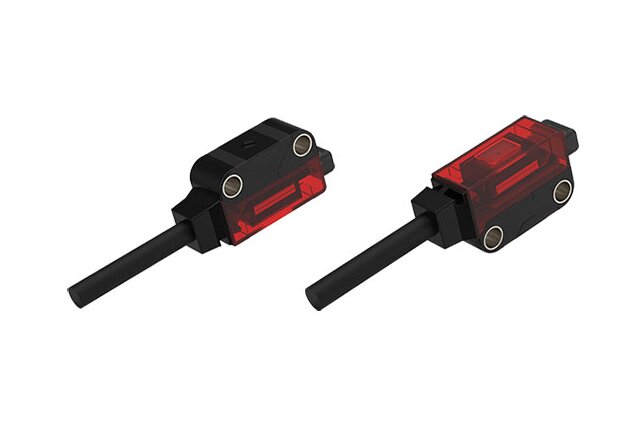
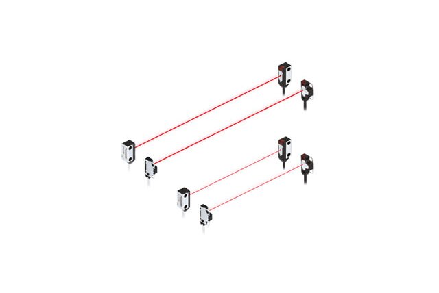
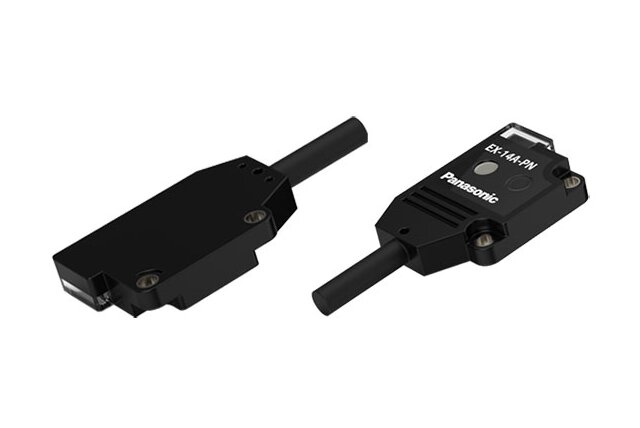
- Ultra‑compact laser sensors (EX‑L200 series)
Provide high-directionality detection through viewports, enabling accurate wafer monitoring from outside the chamber.
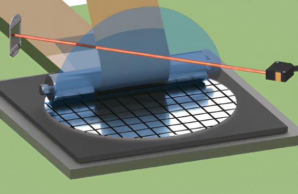
- Laser displacement sensors (LS‑500 series)
Detect small positional deviations with high precision, even at longer distances.
Wafer handling and vacuum robot interaction
Ensuring stable wafer seating during transfer
Inside etching equipment, wafers are transferred between process steps using vacuum robot systems. The correctness of this handling plays a crucial role in overall process stability.
Even small deviations in wafer seating or movement during transfer can introduce variation before the etching process begins. These effects are often subtle and may only become visible in downstream process results.
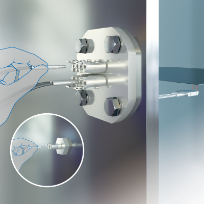
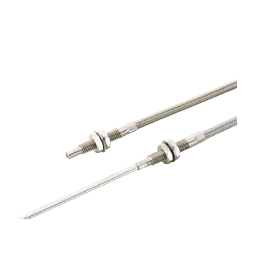
Reliable sensing is therefore required to verify wafer presence and positioning under vacuum conditions without introducing contamination or interference. Fiber optic sensing technologies enable this by providing accurate detection in confined and sensitive environments, supporting stable and repeatable wafer handling.
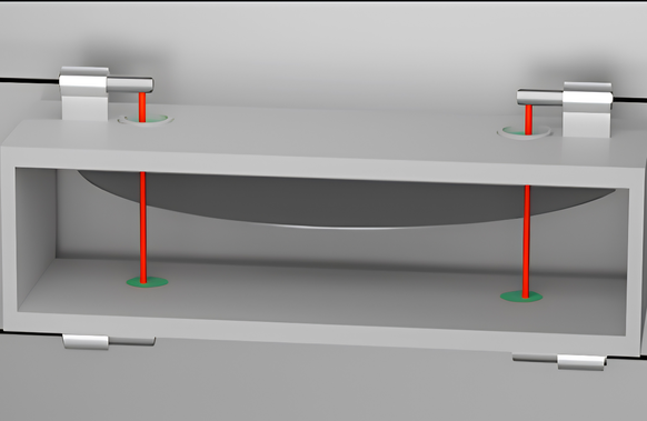
Panasonic solutions
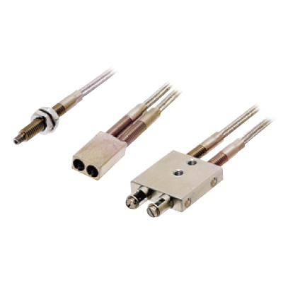
- Fiber optic sensing
Enables non-intrusive detection of wafer presence and positioning in vacuum and chemically sensitive environments.
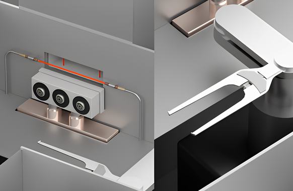
- Compact fiber colutions in vacuum process
Allow stable detection without introducing heat or interference near the wafer
Electrostatic charge control
Preventing process disturbance in dry etching
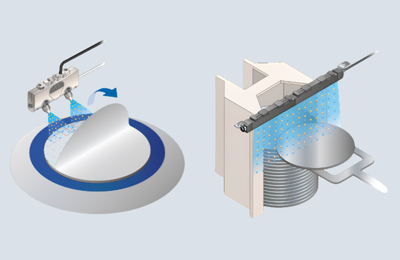
Dry etching processes can generate electrostatic charge, which influences how particles behave and how wafers interact with their surroundings. This can lead to contamination risks or instability if not properly controlled.
Because electrostatic effects build up gradually, they are not always immediately visible. However, their impact on process stability can be significant over time.
By actively neutralising charge during wafer handling and processing, these effects can be reduced. This results in more predictable wafer behaviour, cleaner process conditions and improved consistency across batches.
Panasonic solutions
- Ionizers (ER‑X series)
Neutralize electrostatic charge during wafer handling and processing.
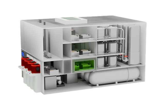
Chemical monitoring and safety in wet etching
Ensuring controlled and reliable process conditions
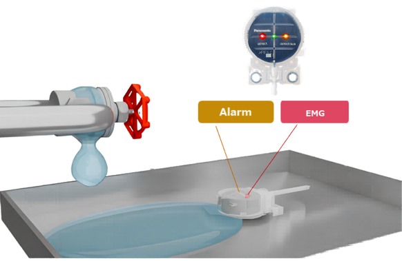
Wet etching relies on aggressive chemicals that must be carefully managed to ensure both process stability and safe operation. Variations in liquid levels, contamination or undetected leakage can quickly affect performance.
At the same time, equipment must comply with strict safety requirements, making continuous monitoring essential. The challenge lies in detecting changes early enough without interrupting the process unnecessarily.
Advanced sensing solutions enable stable monitoring of liquid levels and leakage conditions, even in chemically aggressive environments. By detecting deviations at an early stage, it becomes possible to maintain process continuity while ensuring safe operation.
Panasonic Solutions
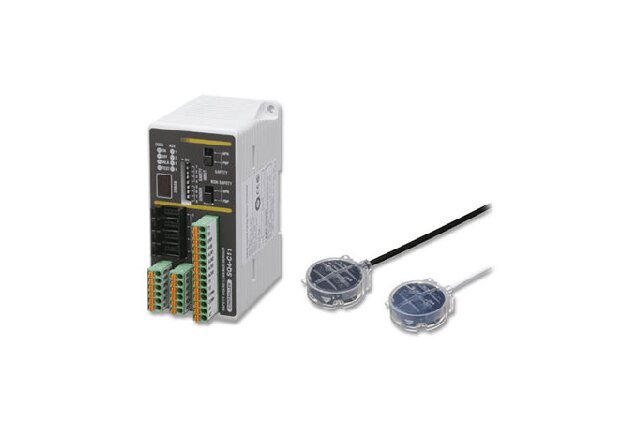
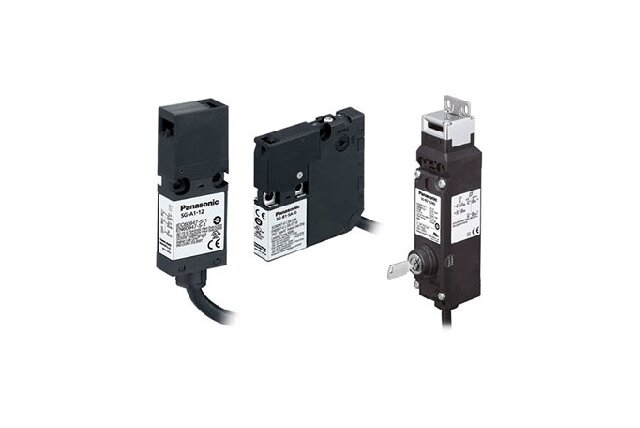
- Leakage sensors (SQ4 series)
Enable two-stage detection (alarm + emergency stop), ensuring both safety and uptime.
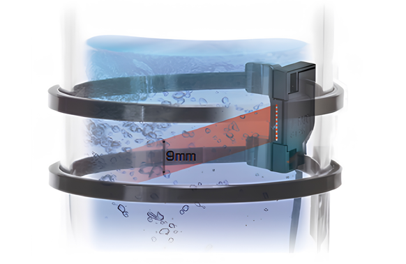
- Liquid level sensors
Provide stable detection of chemical levels without being affected by bubbles or deposits.
Why stability in etching determines downstream performance
The etching process is a decisive step in defining the final device structure. Any variation introduced at this stage is difficult to correct later in the process flow.
Small instabilities can lead to deviations in pattern transfer, changes in etch profiles or increased need for metrology correction. Over time, this can translate into reduced yield and higher process complexity.
This is why etching is not only a material removal step, but a critical control point within the entire front-end process. Ensuring stability here directly supports consistent performance in all downstream steps.
Panasonic Industry solutions for etching processes
Panasonic Industry supports semiconductor equipment builders with:
- compact sensing for vacuum and confined environments
- high-precision laser and displacement sensors
- non-intrusive fiber optic detection
- electrostatic control solutions
- chemical monitoring and safety systems
These technologies enable stable, repeatable and scalable etching processes, from development to high-volume manufacturing.