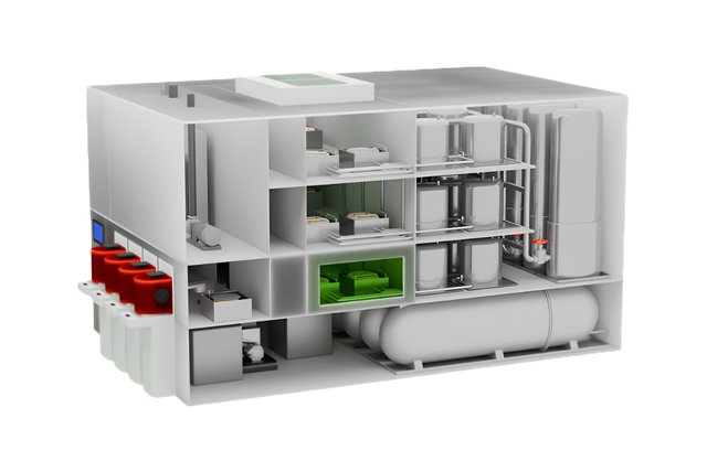
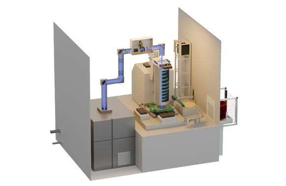
Semiconductor front‑end exposure process - Stability before lithographic accuracy
How handling stability defines lithographic accuracy
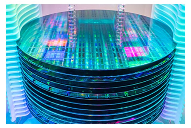
Lithographic exposure is one of the most critical process steps in semiconductor front‑end manufacturing.
During exposure, critical dimensions (CD), overlay accuracy and pattern fidelity are defined. Once this step is completed, downstream processes such as etching and deposition can no longer correct deviations introduced earlier.
This makes stability during exposure preparation and handling essential. Even small variations during wafer or reticle positioning, electrostatic charge buildup or environmental disturbance can propagate into yield loss later in the process flow.
For this reason, exposure tools rely on extremely stable sensing, positioning and safety mechanisms, often operating in:
- space‑constrained layouts
- vibration‑sensitive environments
- temperature‑controlled chambers
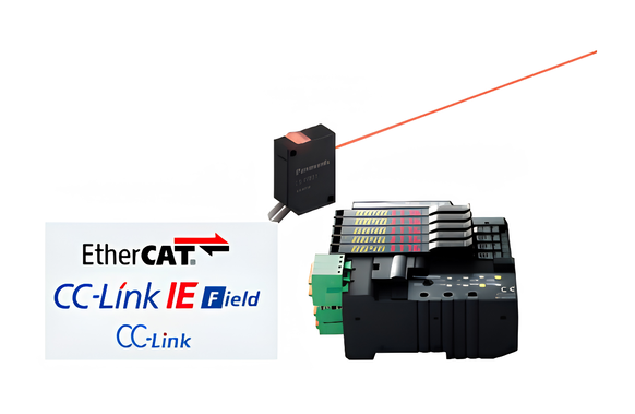
Panasonic Industry supports exposure equipment builders with optical, fiber‑based and safety sensing technologies designed specifically for front‑end lithography environments, where detection must be accurate without influencing the exposure process itself.
What challenges define front-end exposure equipment?
Modern exposure tools must manage several tightly coupled challenges simultaneously:
- Wafer and reticle alignment at micrometer and sub‑micrometer scale
- Reliable detection through sealed chambers and optical viewports
- Electrostatic charge suppression during handling and transfer
- Stable detection close to optics without heat generation or stray light
- Safety‑critical monitoring without increasing tool footprint
The sections below describe the front‑end exposure process step by step, explaining where sensing and safety solutions play a critical role.
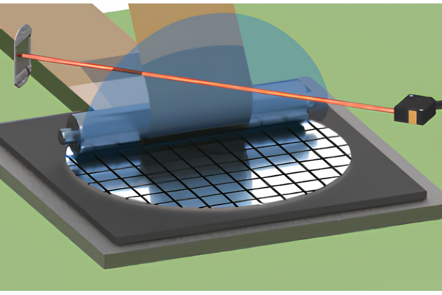
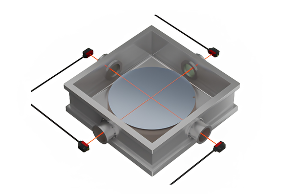
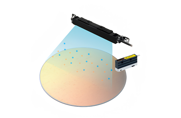
Wafer and reticle alignment
Ensuring positional accuracy before exposure
Accurate alignment of both wafer and reticle is fundamental for achieving overlay accuracy and pattern fidelity during exposure.
Alignment‑related risks
- Misalignment during wafer centering
- Positional drift caused by vibration or temperature variation
- Limited installation space near alignment stages
Panasonic sensing approach
Panasonic Industry supports high‑precision alignment with displacement and laser sensing technologies designed for semiconductor equipment:
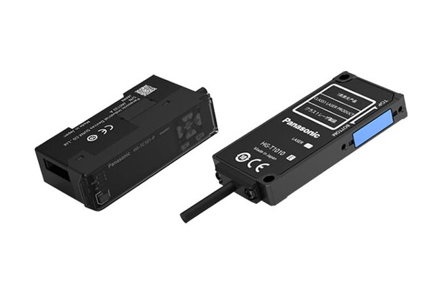
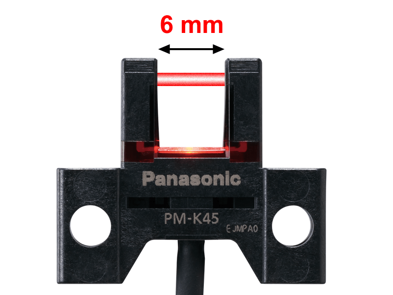
- HG‑T digital displacement sensors
Enable precise notch and eccentricity detection for wafer centering. The line‑beam concept allows stable measurement even with slight positional variation.
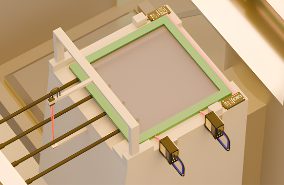
- HL‑G1 / HL‑G2 laser displacement sensors
Provide high‑speed positional feedback for alignment control, suitable for reflective surfaces typically found in lithography environments.
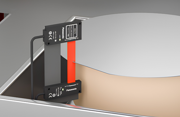
Reticle handling, seating and mapping
Reliable detection without disturbing optical conditions.
Reticle handling requires extremely stable detection, while avoiding heat sources, indicator light or electronic interference near the optical path.
Key risks
- Reticle mis‑seating on robot hands or stages
- Incorrect reticle presence detection
- Local heat or light affecting exposure stability
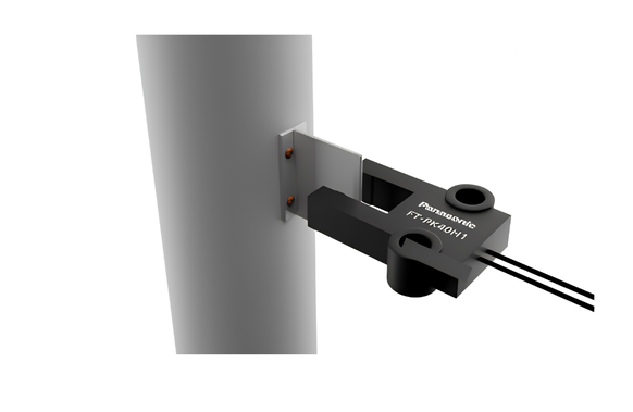
PANASONICSOLUTIONS FOR RETICLE HANDLING
Panasonic fiber‑based sensing enables detection without influencing sensitive exposure conditions:
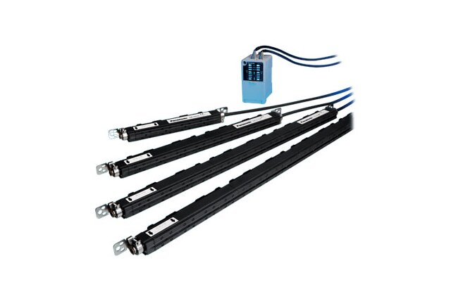
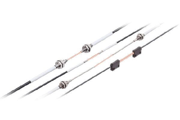
- U‑shaped fiber sensor heads (with remote amplifiers)
No electronics at the sensing point, preventing heat generation and optical disturbance. - Metal‑free, chemical‑resistant fiber heads (FT‑L80Y / FT‑V80Y / FT‑Z802Y)
Provide stable detection even in contaminated or reflective environments.
- LS‑500 amplifier‑separated laser sensors
Detect small reticle displacement or protrusion with flexible installation in tight layouts.
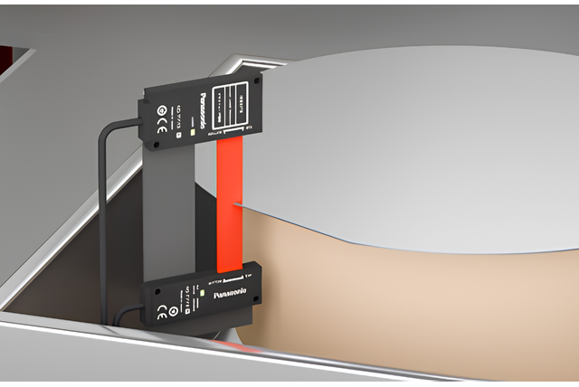
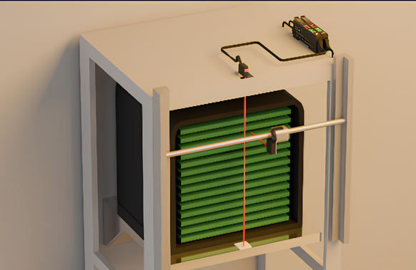
Wafer detection through viewports
Verifying wafer status without opening the chamber.
Exposure tools often require wafer detection through sealed viewports, making stable optical detection critical.
Key challenges
- Limited viewing angles
- Reflections on glass surfaces
- Reduced accuracy with conventional sensors
Panasonic solutions for viewport detection
Panasonic laser sensing technologies enable reliable detection through glass interfaces:
- EX‑L200 ultra‑compact laser sensors
High beam directivity ensures stable detection through viewports while minimizing installation space.
- LS‑500 laser sensors with communication units
Provide high‑precision detection combined with diagnostic feedback for monitoring and optimization.
Electrostatic charge suppression during exposure handling
Preventing distortion and particle attraction.
Electrostatic charge can lead to wafer deformation, particle attraction and unstable handling, all of which directly impact exposure quality.
Key risks
- Wafer distortion during adsorption
- Particle attraction in clean environments
- Uncontrolled electrostatic discharge
Panasonic solutions for static control
Panasonic Industry provides ionization and monitoring technologies for controlled electrostatic conditions:
- ER‑X pulsed AC ionizers
Neutralize electrostatic charge across larger areas. - ER‑V compact ionizers
Suitable for integration in space‑constrained exposure modules. - EF‑S1 surface potential sensors
Enable visualization and verification of residual charge levels.
Leak detection and liquid monitoring in exposure tools
Protecting uptime and operational safety
Cooling circuits and controlled liquids are essential for exposure tools, and must be monitored continuously.
Key risks
- Undetected leaks leading to tool downtime
- Safety risks due to abnormal liquid conditions
- Incorrect liquid levels affecting process stability
Panasonic solutions for safety and monitoring
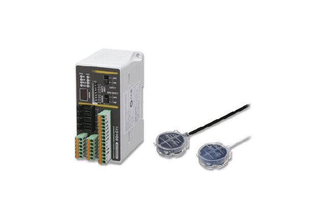
- SQ4 safety leakage sensors
Thru‑beam detection with two‑stage output (early warning + emergency stop), supporting SEMI S2 and high safety levels.
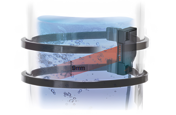
- EX‑F1 / FD‑F series liquid level sensors
Metal‑free, chemical‑resistant sensing for stable level detection independent of bubbles or deposits.
Why Panasonic Industry for exposure equipment
Panasonic Industry supports front‑end exposure equipment builders with:
- Deep application knowledge in semiconductor front‑end processes
- Compact sensing solutions suited for space‑critical tools
- Optical and fiber‑based detection that does not disturb lithographic conditions
- Connectivity options supporting diagnostics and predictive maintenance