Semiconductor automation solutions for front‑end and back‑end manufacturing
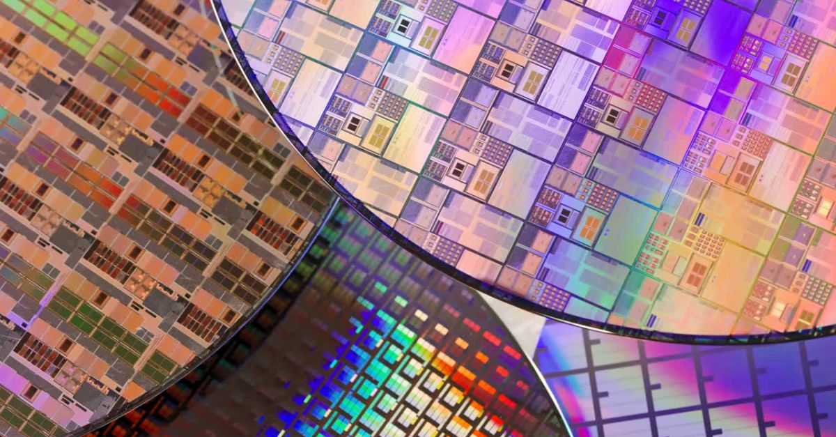
The semiconductor industry is defined by extreme precision, ultra‑clean processes and continuously shrinking form factors. From wafer fabrication to back‑end assembly and testing, semiconductor manufacturing equipment must operate reliably at nanometer‑level accuracy.
Panasonic Industry provides sensor, automation and motion solutions for semiconductor manufacturing equipment, supporting both front‑end and back‑end processes such as wafer handling, inspection, positioning and final assembly.
Our technologies are used by semiconductor equipment builders worldwide to enable compact machine designs, stable wafer detection and reliable automation in space‑constrained and high‑precision environments.
Semiconductor manufacturing: front‑end and back‑end processes

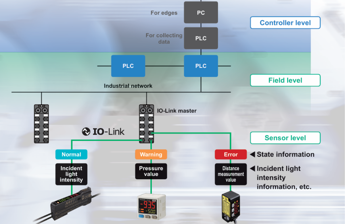
Behind every semiconductor tool are countless technical details that determine performance, yield and uptime.
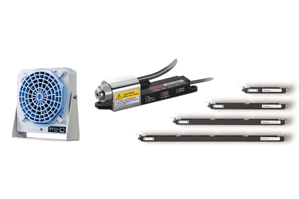
Panasonic Industry focuses on the critical functional elements inside semiconductor manufacturing machines, from precision sensing and motion control to safety and static control, enabling equipment builders to meet the demands of high‑performance semiconductor production environments.
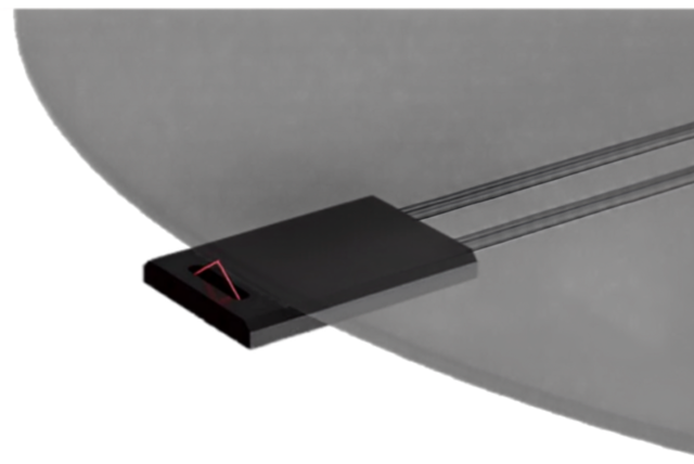
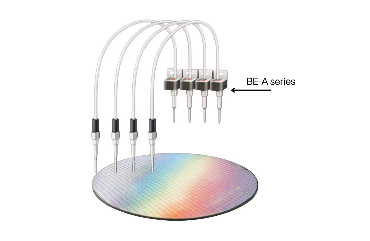
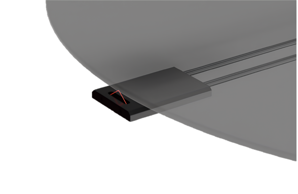
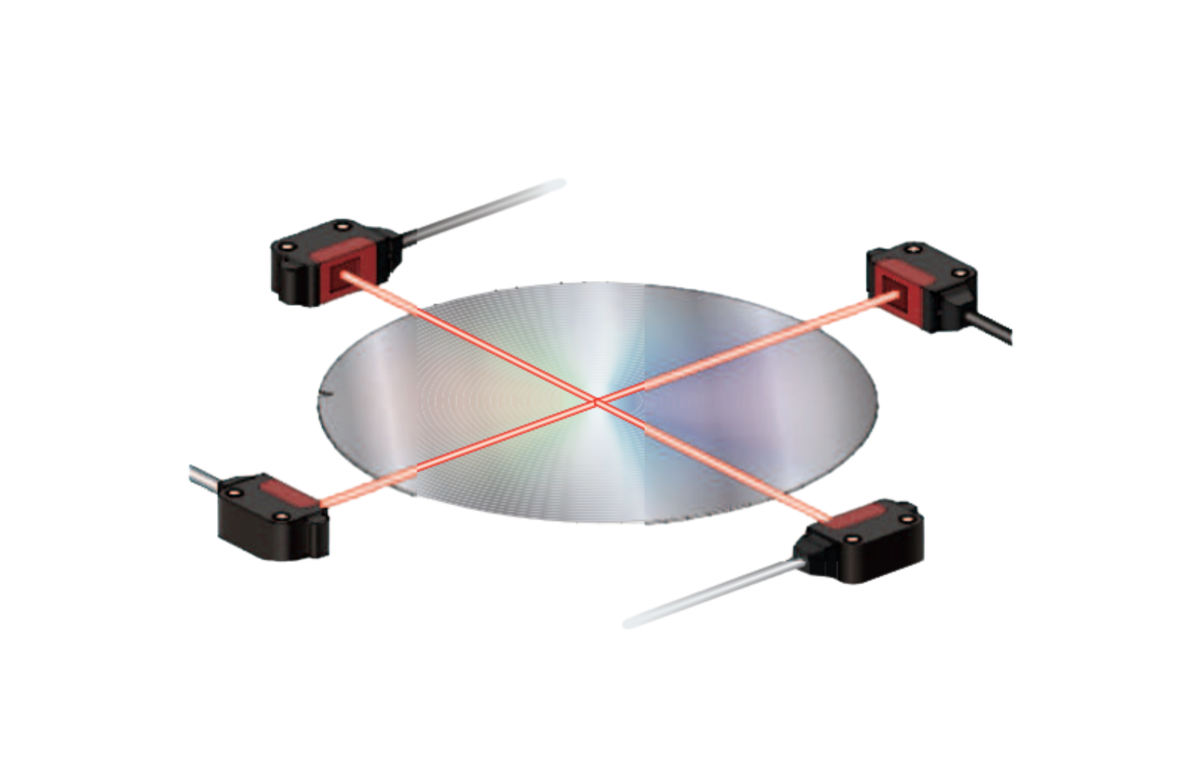
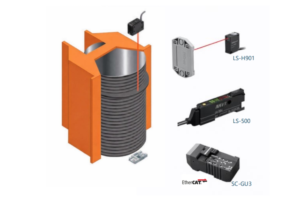
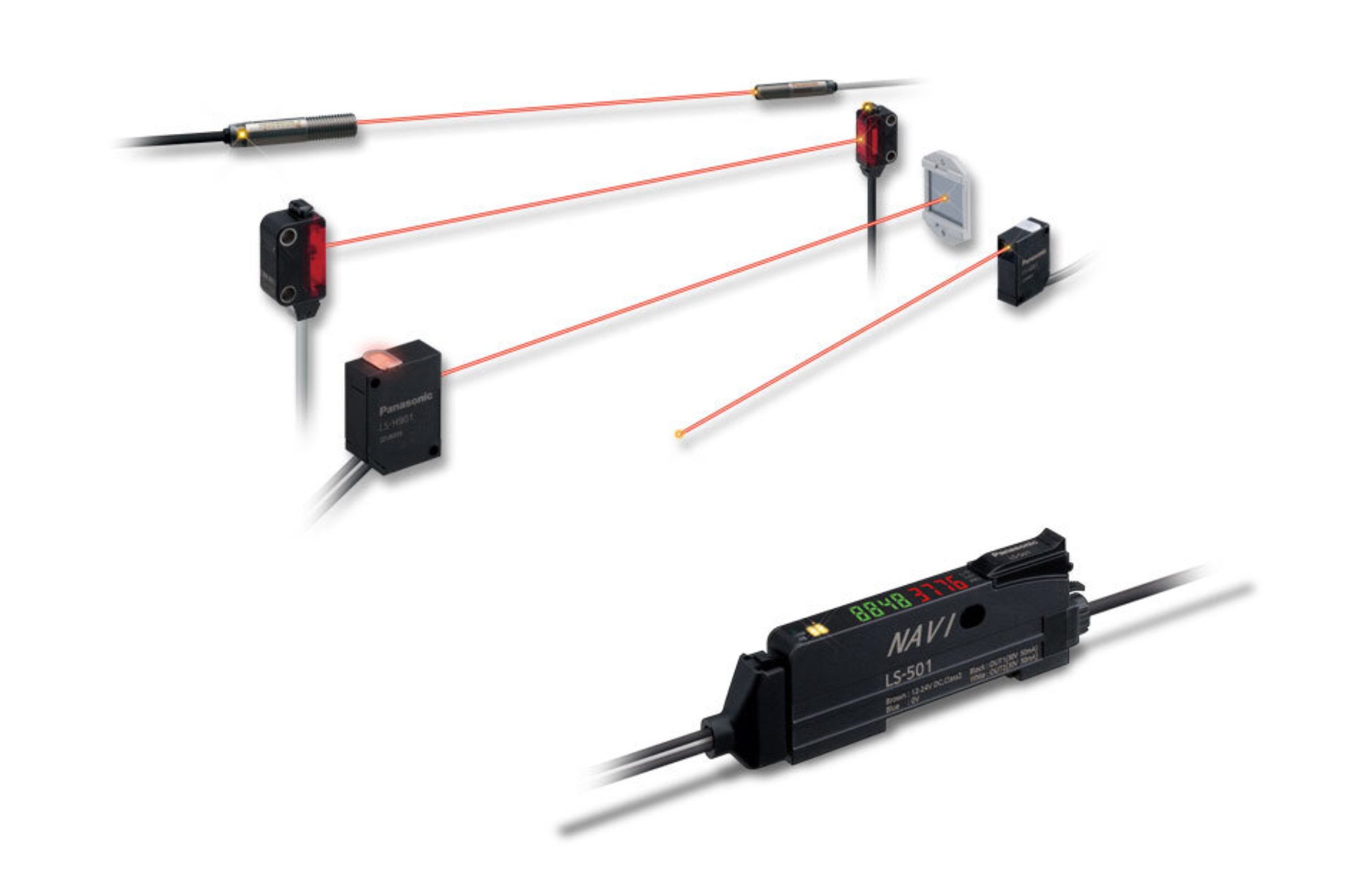
Front‑end semiconductor manufacturing: precision sensing and control
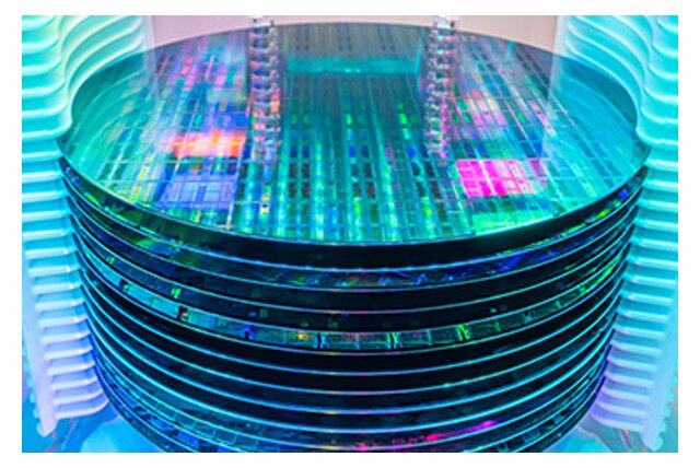
In front‑end semiconductor manufacturing, wafers are processed layer by layer in ultra‑clean and highly controlled environments. Processes such as lithography, deposition and etching demand stable positioning, accurate detection and vibration‑controlled motion.
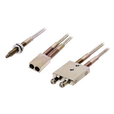
Panasonic Industry supports front‑end semiconductor equipment with high‑precision sensors, measurement technologies and motion solutions designed for cleanroom compatibility and compact tool architectures.
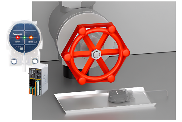
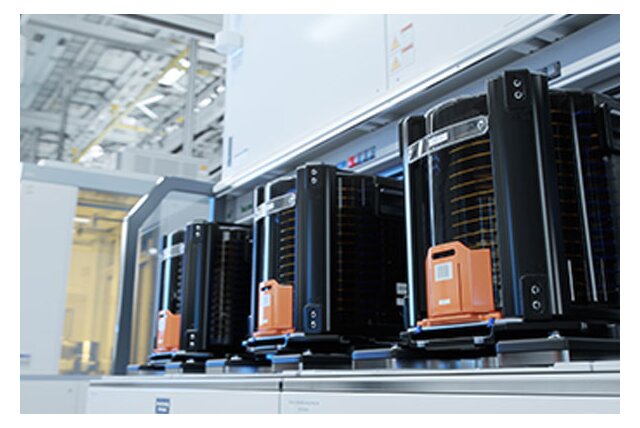
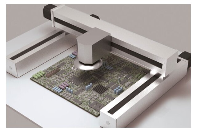
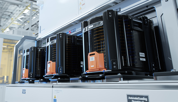
Back‑end semiconductor processing: assembly, testing and packaging
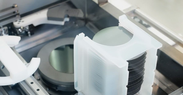
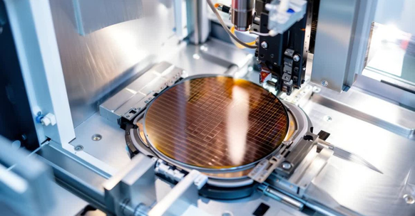
During back‑end semiconductor processing, wafers are singulated into individual dies and prepared for assembly, testing and packaging. These stages require reliable wafer and die handling, precise positioning and repeatable detection inside compact and high‑speed automation systems.
Panasonic Industry solutions support back‑end equipment builders in designing reliable, space‑efficient automation platforms that meet throughput and quality requirements.
Semiconductor Insights: unpacking semiconductor technology
The Semicon Insights blog series explores practical sensing, motion and automation challenges in semiconductor manufacturing. Topics include:
- wafer handling and detection
- precision measurement and inspection
- compact sensing for space‑constrained tools
- reliability in front‑end and back‑end processes
By focusing on real equipment challenges, Semicon Insights supports engineers and designers working on next‑generation semiconductor tools.