Ready-to-integrate solutions for semiconductor equipment builders
Engineered for your process. Delivered ready to integrate.
In semiconductor equipment development, the real challenge is rarely sourcing components. The challenge is integrating them into the machine quickly, correctly and consistently.
Engineering teams spend valuable time adapting cable lengths, mounting connectors, configuring devices, labeling components, validating quality requirements and preparing products for installation. These tasks are essential, but they do not create competitive differentiation.
Panasonic helps reduce this effort by delivering sensors, motion components and assemblies prepared according to your exact requirements and ready for integration into the final machine.
Why integration becomes the bottleneck
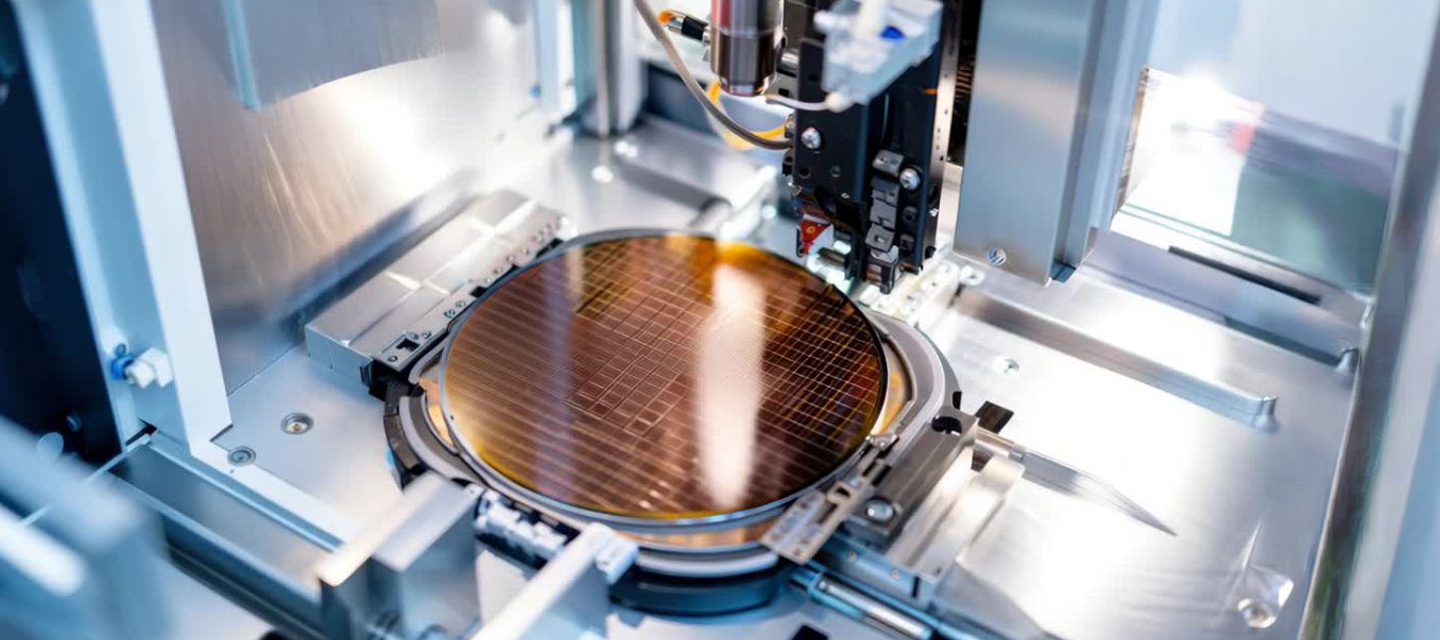
Semiconductor OEMs operate under a unique set of constraints. Equipment must be designed within extremely limited spaces, such as EFEM modules, load ports and robot arms, while still operating reliably in demanding environments that may involve vacuum conditions, high temperatures or aggressive chemicals.
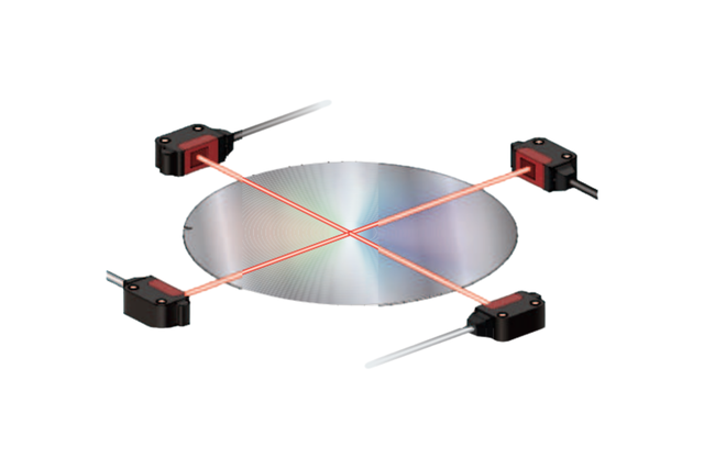
At the same time, wafers are becoming thinner and more fragile, requiring highly stable detection and handling. Combined with increasing pressure on engineering resources and shorter development cycles, this creates a situation where standard components no longer provide a sufficient starting point.
What is needed is not just a product, but a solution that is already adapted to the application context.

What ready-to-integrate really means
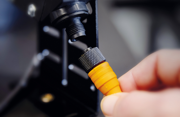
Customization is often understood as modifying a component. In semiconductor equipment, however, it goes further than that.
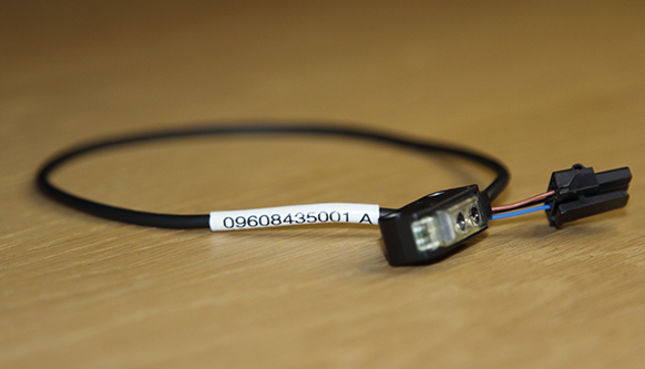
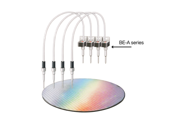
It is about preparing components in such a way that they can be integrated directly into the machine, without additional engineering steps. This includes assembling sensors with mounting hardware, configuring sensors, PLCs or HMIs in advance, and adapting cabling and connectors to match the exact requirements of the system.
In addition, components are labeled correctly for traceability and delivered in a way that supports efficient installation. Testing can be extended to include specific electrical and mechanical requirements, ensuring that the product performs as expected in its final environment.
The result is a significant reduction in manual work during machine build and commissioning, and a more predictable integration process.
Prepared for semiconductor manufacturing
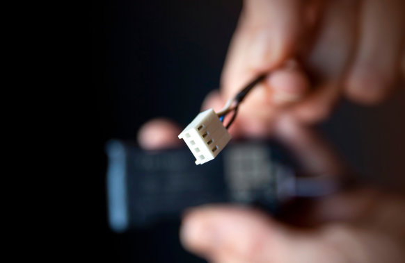
Customization becomes particularly valuable when aligned with the realities of semiconductor manufacturing.
In wafer handling systems such as EFEMs and load ports, where space is limited and precision is critical, pre-configured and correctly labeled components reduce installation errors and support stable operation from the first machine build. Semiconductor equipment builders can receive sensors, motion components and assemblies prepared exactly according to system requirements, reducing engineering effort during integration.
In process tools such as cleaning, CMP and diffusion equipment, reliability and consistency are essential. Components can be cleaned and packed according to customer requirements and supplied with the required documentation and quality controls. This helps maintain process cleanliness, improve traceability and ensure repeatable quality across production volumes.
Typical semiconductor customization options include:
- Customized cable lengths
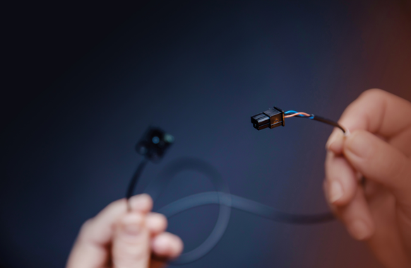
- Connector installation and validation
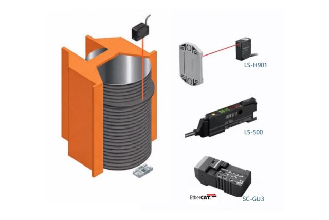
- Sensor pre-configuration and parameter setting
- Product cleaning and packaging according to customer requirements
- Additional quality inspections and testing
- Customer-specific labeling for traceability
- Pre-assembled product sets for faster machine build
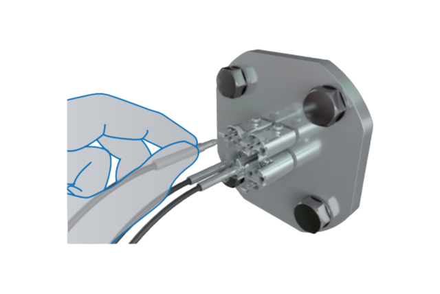
By transferring these activities from the machine builder to a controlled customization process, installation effort is reduced while product consistency increases. Connector mounting, for example, is combined with dedicated quality checks, eliminating the need for specialized tools and validation resources within the machine builder's own production process
As systems move from prototype to series production, the benefits extend further. Pre-assembly and optimized packaging support faster system build, while maintaining consistency across multiple machines.
Motion customization for semiconductor equipment
Motion systems play a critical role in wafer handling, robotics, positioning and process automation. Just like sensors, motion components can be prepared and delivered in a configuration that simplifies integration and reduces engineering workload.
Customization options include:
- Servo motors with customer-specific cable lengths
- Connector mounting and validation
- Pre-assembled motor and gearbox combinations
- Motion controller configuration support
- Product cleaning and packaging according to customer requirements
- Customer-specific labeling and traceability
For applications requiring fast acceleration, high positioning accuracy and high torque at low speeds, a servo motor can be supplied together with a planetary gearbox as a complete assembly. This creates a compact and efficient motion solution while reducing mechanical integration effort during machine build.
By receiving a ready-to-install assembly instead of multiple separate components, semiconductor equipment builders reduce sourcing complexity, assembly time and commissioning effort.
From requirement to repeatable delivery
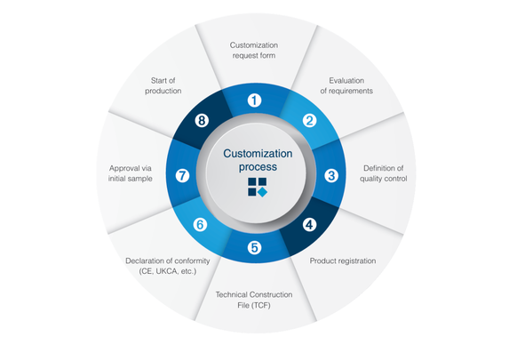
To deliver this level of reliability, customization follows a defined and controlled process rather than ad hoc engineering.
Starting from clearly defined technical requirements, solutions are evaluated together with engineering teams and aligned with the necessary quality standards. Each product is then documented, registered and validated, including the creation of a Technical Construction File where required.
Compliance and certification are addressed early, and first samples are approved before moving into series production. This ensures that customized products are not only tailored to the application, but also consistent and repeatable at scale.
Why this matters for semiconductor equipment builders
For machine builders, the impact of customization goes beyond convenience. It directly influences engineering efficiency, system reliability and time-to-market.
Reducing integration effort allows engineering teams to focus on system-level challenges rather than component adaptation. Avoiding wiring errors and installation issues improves first-time-right performance. Faster commissioning accelerates qualification, while consistent product preparation supports scaling across global production.
In this way, customization becomes a practical tool to bridge the gap between design and production.