
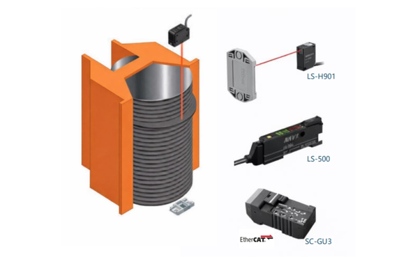
Our products in semicon applications: LS-500 series
In high‑precision semiconductor manufacturing, wafer handling accuracy is critical. Even the smallest deviation in wafer position can lead to mis‑picks, collisions, rejects, and costly downtime. One of the most effective ways to prevent these issues is protrusion detection, verifying whether a wafer is sticking out of its slot beyond the allowed tolerance.
Why protrusion detection matters
As wafer diameters increase and materials diversify, handling robots face tighter requirements. A protruding wafer of just a fraction of a millimeter can have major consequences:
- Mechanical interference during picking
- Increased risk of wafer edge damage
- Lower overall tool availability
- Higher operational cost due to stopped processes or scrapped wafers
To maintain reliability, fabs depend on highly stable, highly repeatable sensors capable of detecting minimal deviations, regardless of wafer material or reflectivity.
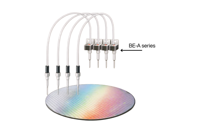
Proven performance: Panasonic LS‑H901 (LS‑500 Series)
During recent application testing, the Panasonic LS‑H901 confirmed its exceptional performance in protrusion detection tasks. The sensor demonstrated stable detection across various wafer types, including:
- Silicon
- Glass / transparent wafers
- SiC (Silicon Carbide) wafers
The key: its coaxial retro‑reflective optical principle, which ensures consistent results even in the most challenging conditions.
What is coaxial retro‑reflective sensing?
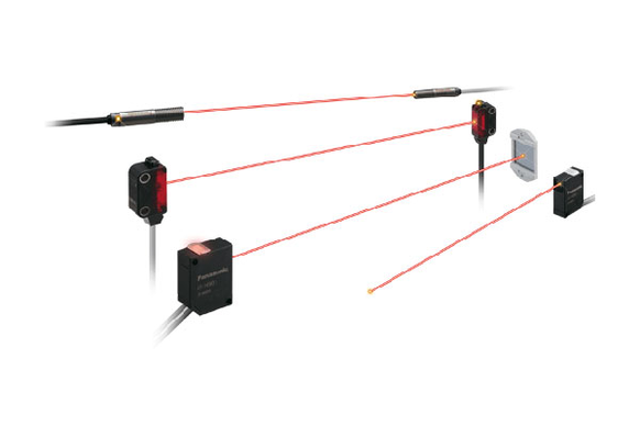
In a coaxial retro‑reflective setup, the sensor emits and receives light along the same optical axis. A dedicated reflector returns the beam to the receiver.
This configuration offers significant advantages for semiconductor applications:
Key Benefits
- Reliable detection on difficult surfaces
Works even with transparent or highly reflective wafer materials. - Low sensitivity to wafer tilt or angle
Minimizes false detections caused by slight misalignment. - Compact sensor head
Simplifies integration into tight end‑effector or FOUP/SMIF environments. - High repeatability
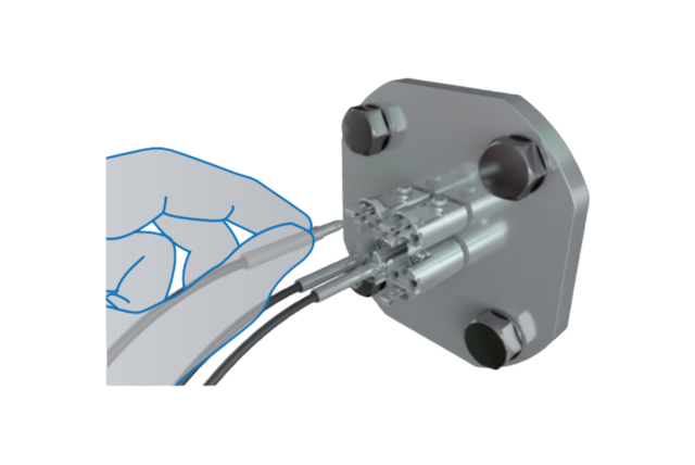
Essential for detecting very small height or position deviations. - Quick, repeatable setup
Through the LS‑500 amplifier with intuitive configuration.
Industry 4.0 ready: intelligent monitoring via EtherCAT
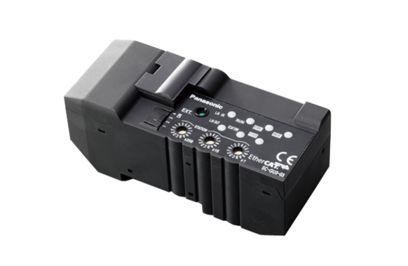
By adding the SC‑GU3 EtherCAT communication module, users gain:
- Remote sensor presetting and configuration
- Real‑time monitoring
- Predictive maintenance possibilities
- Seamless integration into PLC or PC environments
This makes the LS‑H901 not only precise, but also fully connectable for modern semiconductor equipment.
How to detect wafer inclination during transfer – key questions answered
|
Why is wafer inclination difficult to detect during transfer?
|
Wafer inclination is difficult to detect because it typically occurs while the wafer is moving, rather than when it is stationary. Most conventional sensors are designed to detect presence only and do not capture deviations in alignment or angle. As a result, small inclinations during transfer often remain unnoticed until they lead to process variation or mechanical contact later in the tool.
|
|
What causes wafer tilt in semiconductor handling systems?
|
Wafer tilt is usually the result of small mechanical and positioning variations within the handling system. These can originate from slight misalignment during pick-and-place, tolerances in robot mechanics, or variations in wafer positioning inside carriers such as FOUPs. Because these effects occur dynamically during motion, they are not always visible or detectable with standard sensing approaches.
|
|
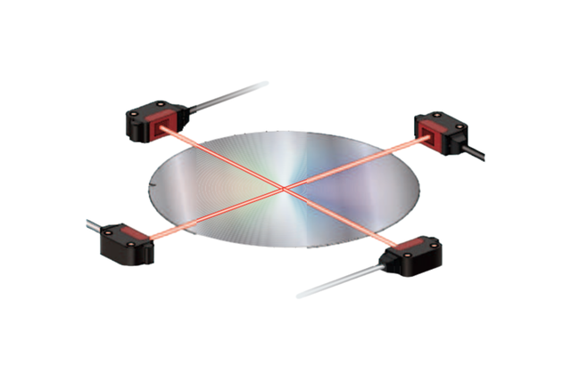
How can laser sensors detect wafer inclination in motion?
|
Laser-based displacement sensors can detect wafer inclination by continuously measuring the position of the wafer while it is moving. Instead of simply confirming whether a wafer is present, they provide precise distance information that makes it possible to identify even small angular deviations. This allows wafer tilt or misalignment to be detected in real time, before the wafer reaches the next process step.
|
|
Why is early detection critical to prevent wafer damage?
|
Early detection is critical because wafer inclination can quickly result in mechanical contact with tool surfaces or misprocessing in subsequent steps. Once a tilted wafer enters a sensitive process module, the risk of damage or yield loss increases significantly. By detecting inclination during transfer, it becomes possible to correct or reject the wafer at an early stage, which helps prevent damage and improves overall process stability.
|