Detecting skew in glass panel wafer handling
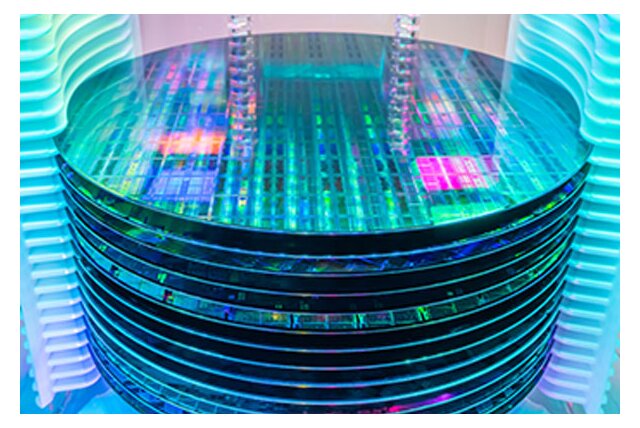
As semiconductor architectures evolve towards chiplet integration and advanced packaging, glass panel wafers are becoming increasingly relevant. These substrates enable larger form factors and new integration concepts, but they also introduce new handling challenges.
One of these challenges is skew detection during transfer.
When a glass panel wafer is slightly misaligned or rotated during handling, it can result in:
- misplacement at the next process step
- contact errors in equipment
- increased risk of breakage or yield loss
Unlike traditional silicon wafers, glass panel substrates are often larger, thinner and more sensitive to mechanical misalignment. Detecting skew early in the transfer process becomes critical to maintaining stability across the equipment.
The challenge: detecting skew during wafer transfer
In EFEM systems and handling modules, wafers are transferred at high speed using robot arms or end-effectors. During this motion, small angular deviations (skew) are not always visible, but they can introduce variation in downstream processes.
Detecting this skew is challenging because installation space on end-effectors is extremely limited. The detection must not interfere with wafer movement and the system must detect small deviations reliably and consistently.
This requires sensing solutions that are both compact and precise, while remaining stable in dynamic conditions.
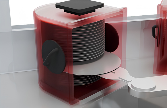
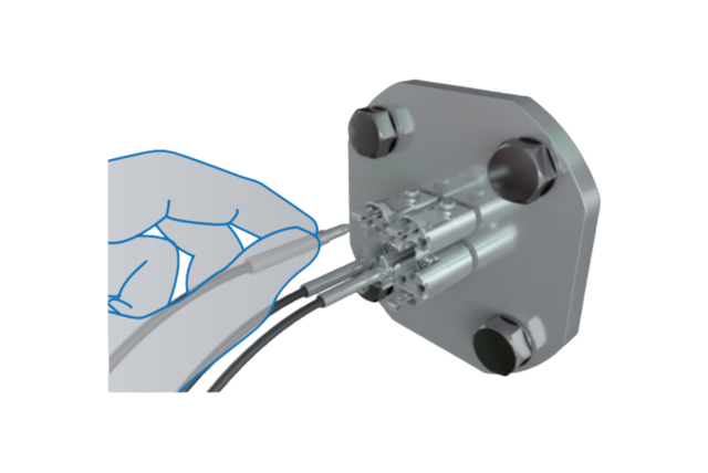
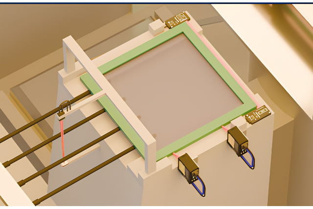
A practical solution: fiber optic skew detection
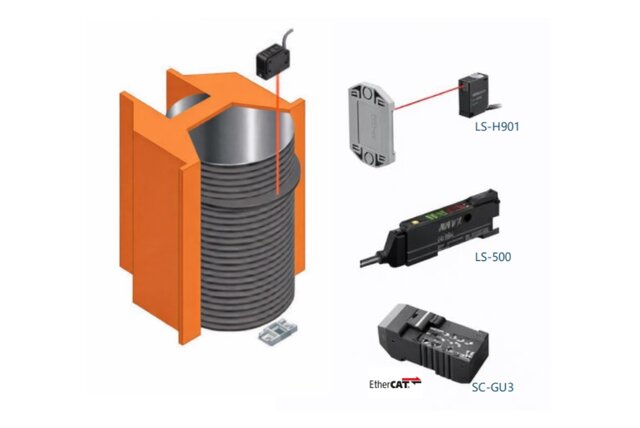
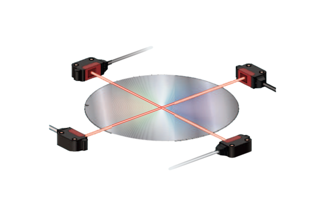
A proven approach is the use of dual fiber optic sensors mounted on both sides of the end-effector.
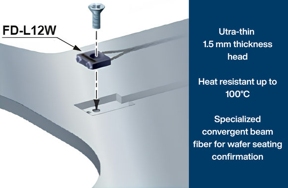
By integrating FD‑L12W ultra-compact fiber heads with an FX‑501 digital amplifier, it becomes possible to detect wafer position on both sides simultaneously.
This setup allows:
- comparison of wafer position on both ends
- early detection of angular deviation (skew)
- real-time feedback during transfer
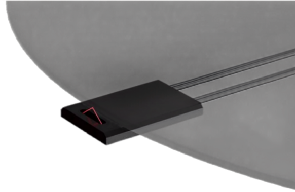
The key advantage of this solution is the smallest-in-class sensing head footprint, enabling integration directly into space-constrained robot hands.
Why compact sensing matters in EFEM systems
In semiconductor handling equipment, space is always limited, especially at the end-effector.
The FD‑L12W fiber head is designed for ultra-compact installation, precise and localized detection. The fiber head also has minimal interference with surrounding structures
Combined with the FX‑501 amplifier, the system provides stable detection performance, flexible adjustment and signal processing, and has a reliable operation across different wafer types
This makes it suitable not only for glass panel wafers, but also for other applications requiring precise wafer detection.
Why early skew detection improves process stability
In semiconductor manufacturing, variation rarely starts where it is detected.
A small misalignment during transfer can later result in positioning errors in bonding or testing, mechanical stress in downstream tools and yield loss that is difficult to trace back.
By detecting skew directly at the handling stage, these risks can be mitigated early.
This supports more stable wafer transfer, reduced downstream variation and improved overall equipment reliability.
Supporting next-generation semiconductor handling
As semiconductor processes move towards larger substrates and more complex packaging structures, handling precision becomes increasingly critical.
Applications such as glass panel wafer transfer require:
- compact sensing solutions
- non-intrusive detection
- real-time feedback
Panasonic Industry supports these requirements with a broad range of sensing technologies, including fiber optic sensing solutions designed for integration in confined and demanding environments.
FAQ
|
Why is skew detection important in semiconductor wafer handling? |
Skew detection is important because even small angular misalignments during wafer transfer can lead to positioning errors in downstream processes such as bonding, inspection or testing. Detecting these deviations early helps prevent yield loss and equipment instability. |
|
What makes glass panel wafers more challenging to handle? |
Glass panel wafers are typically larger, thinner and more fragile than traditional silicon wafers. This makes them more sensitive to mechanical stress and alignment errors during handling, especially in high-speed transfer systems. |
|
Why is skew difficult to detect in EFEM systems? |
Skew detection is difficult because end-effectors in EFEM systems have very limited installation space. Sensors must be compact and non-intrusive while still being able to detect small positional differences during dynamic movement. |
|
How do fiber optic sensors enable skew detection? |
By placing two compact fiber optic sensors on both sides of the wafer, it is possible to compare position differences in real time. This allows early detection of angular deviation without interfering with wafer transfer. |
|
How does early skew detection improve process stability? |
Early detection prevents alignment issues from propagating to later steps. By identifying deviations during handling, engineers can reduce downstream variation, avoid mechanical stress and improve overall equipment reliability. |
|
How does this solution support advanced semiconductor processes? |
As semiconductor manufacturing evolves towards chiplet architectures and larger substrates, precise handling becomes more critical. Compact sensing solutions enable accurate detection without impacting equipment design, supporting next-generation processes. |