
Compact fiber sensing for semiconductor wafer handling
Sensing challenges in modern semiconductor equipment
In semiconductor wafer handling equipment, available installation space is becoming increasingly limited. Robot arms, end‑effectors and front‑end handling modules are continuously optimized to become thinner, lighter and more compact, while maintaining stable and repeatable wafer detection.
For semiconductor equipment builders, this creates a growing challenge:
how to integrate reliable sensing solutions in tight mechanical designs without compromising performance, clean integration, or future scalability.
As fabs and OEMs continue to push for higher throughput and compact tool designs, sensing solutions must evolve accordingly.
The application challenge: limited space inside wafer handling systems
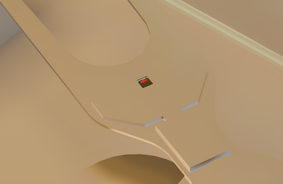
Inside wafer handling machines, sensors are often mounted directly on or near robot arms and end‑effectors, close to the wafer transfer point. In these areas:
- available mounting space is extremely limited
- sensor heads and fibers must be as thin as possible
- amplifiers must fit into compact control cabinets or moving axes
- next‑generation tool designs demand smaller and cleaner sensor integration
In modern semiconductor equipment, compact form factors are no longer a design preference, they are a functional requirement.
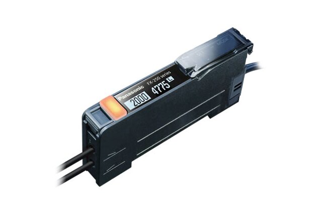
Compact amplification for space‑critical semiconductor applications
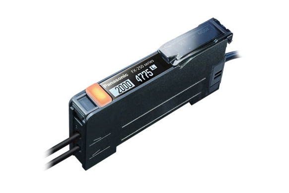
To support these requirements, Panasonic Industry developed the FX250 fiber amplifier for space‑constrained industrial and semiconductor applications.
With a short body length of approximately 46 mm, the FX250 is designed to support equipment builders transitioning toward next‑generation compact architectures, while maintaining practical electrical and mechanical integration.
For semiconductor machine builders, this provides:
- simplified integration in dense electrical layouts
- minimal impact on existing cabinet and wiring designs
- greater freedom in compact mechanical system design
- a future‑ready amplifier footprint aligned with evolving tool architectures
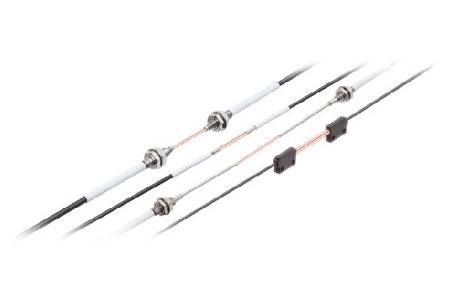
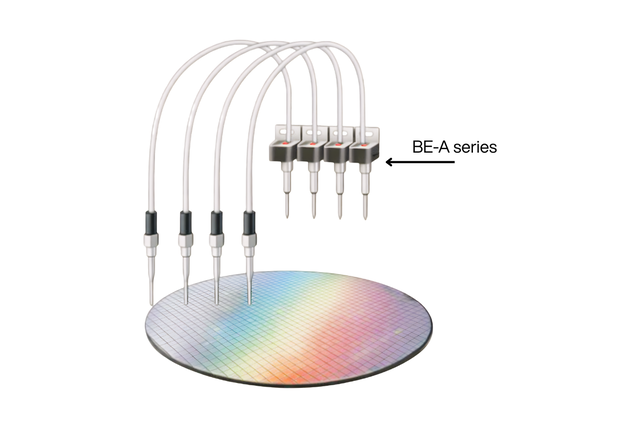
Ultrathin fiber design for modern wafer handling
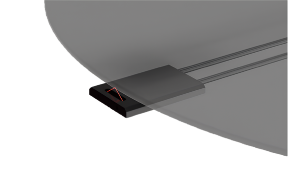
In wafer handling applications, the fiber diameter often has a greater impact than the amplifier itself. Thin fibers are essential to:
- route sensors through narrow robot arms
- reduce mechanical interference near the wafer
- support clean and organized cable routing
- enable compact end‑effector designs
Panasonic Industry’s ultrathin fiber, with a diameter of approximately 1.5 mm, is specifically suited for these space‑limited semiconductor environments.
While the dimensional difference may seem small, in wafer handling systems every millimeter matters. This reduced fiber diameter can be the difference between seamless integration and mechanical compromise.
Combined with the FX250 fiber amplifier, this solution enables precise and stable detection in locations where conventional fiber sensors are difficult to integrate.
Typical use cases in semiconductor wafer handling equipment
The combination of a compact fiber amplifier and ultrathin fiber is well suited for applications such as:
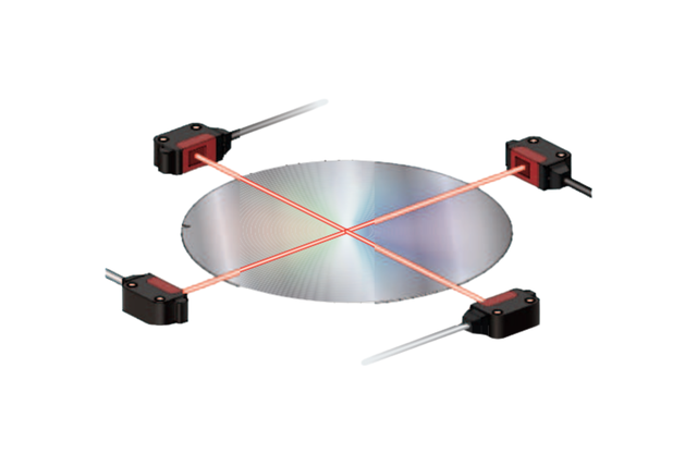
- wafer presence detection on robot arms
- verification of successful wafer pick or place
- position confirmation during wafer transfer
- sensing inside narrow end‑effector assemblies
- space‑critical detection tasks in front‑end or back‑end handling modules
By addressing both amplifier size and fiber thickness, Panasonic Industry supports semiconductor equipment designs that align with the industry’s ongoing miniaturization trends.
FAQ – Compact fiber sensing
|
Why is sensing in wafer handling systems challenging?
|
Sensing in wafer handling systems is challenging because space is limited and environmental conditions are highly controlled. Sensors must operate reliably without interfering with the process, while still detecting wafers accurately during high‑speed movement. Even small disturbances or incorrect positioning can affect downstream processes.
|
|
Why are compact sensors important in semiconductor equipment?
|
Compact sensors are important because semiconductor equipment is designed with extremely tight mechanical layouts. There is often very little room available near robot arms, transfer stages or process modules. Using smaller sensing solutions allows engineers to integrate detection closer to the process without redesigning the machine or compromising performance.
|
|
How do fiber optic sensors enable detection in confined spaces?
|
Fiber optic sensors enable detection in confined spaces by separating the sensing tip from the electronic components. The sensing head can be made very small and placed exactly where detection is needed, while the amplifier is positioned elsewhere. This makes it possible to achieve precise detection in locations where conventional sensors would not fit.
|
|
Why is non-intrusive detection critical in wafer handling?
|
Non-intrusive detection is critical because wafer handling takes place in environments where contamination, heat or light interference must be avoided. Sensors that influence the environment can introduce variation that affects process stability. Fiber optic sensing allows detection without adding heat or electrical interference near the wafer.
|
|
How does compact fiber sensing improve process stability?
|
Compact fiber sensing improves process stability by enabling consistent and repeatable wafer detection, even in complex or constrained environments. Reliable detection of wafer position and presence ensures that subsequent process steps receive the wafer under the correct conditions, reducing variation and improving overall equipment performance.
|