
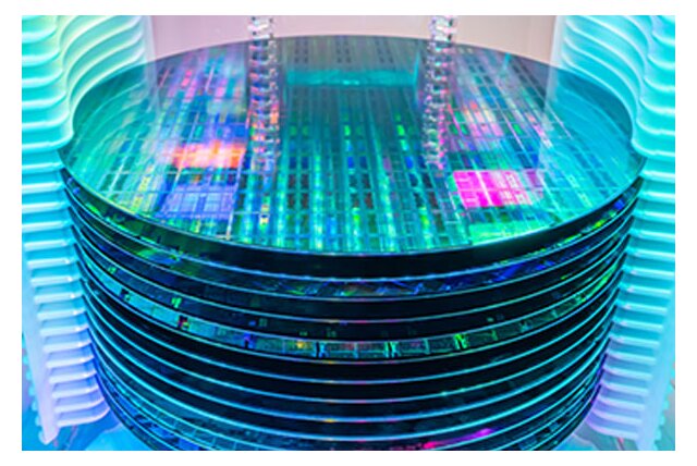
Wafer inclination detection
In advanced wafer handling and inspection, even minimal wafer tilt can affect process stability. That’s why reliable, repeatable wafer inclination detection is becoming an essential function in modern semiconductor equipment.
Why wafer inclination detection matters in semiconductor equipment
As semiconductor manufacturing continues to push the limits of precision, equipment builders face a familiar challenge: tiny deviations can cause outsized problems. Wafer handling is one of the clearest examples, misalignment and tilt can lead to mis-picks, collisions, rejects and unplanned downtime, all of which directly affects tool availability and cost of ownership.
In this environment, inclination detection is not a “nice-to-have.” It is a practical way to maintain process stability, especially in high-speed automation environments where repeatability matters as much as detection accuracy.
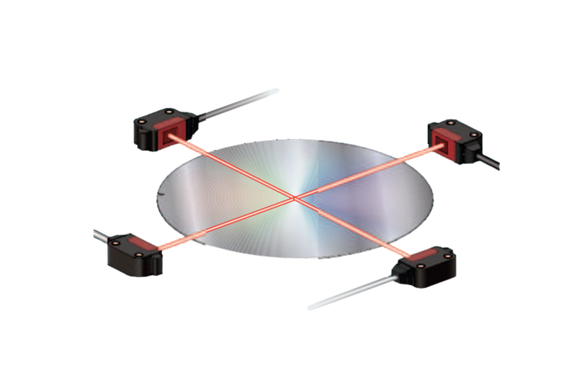
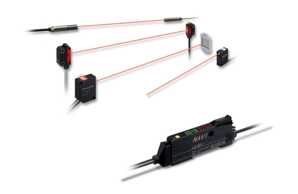
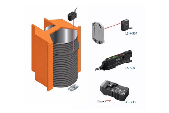
A proven approach: LS-H102 thru beam sensor + LS-500 amplifier
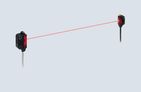
For wafer inclination detection and workpiece orientation monitoring, the LS‑H102 sensor head is part of Panasonic’s LS‑500 digital laser sensor family.
The LS‑H102 is a thru‑beam type laser sensor head with a 1 m sensing range and IP67 protection, making it suitable for robust integration into equipment environments where reliability and uptime are key.
The LS‑500 series documentation explicitly lists the LS‑H102 for wafer inclination detection, reflecting its intended use in semiconductor-related sensing scenarios.
Key benefits for wafer inclination detection
In wafer inclination applications, the LS‑H102 + LS‑500 combination is designed to support stable and repeatable monitoring:
- Stable detection across the wafer surface: helpful for consistent monitoring even when handling conditions vary.
- High repeatability for reliable tilt and orientation monitoring: supporting consistent decision-making in automated handling sequences.
- Compact sensor head for easier integration: the LS‑500 series emphasizes compact head design and straightforward alignment support (visual spot guidance), helping reduce installation complexity.
Together, these characteristics help semiconductor equipment manufacturers improve stability in handling steps where small deviations can have big consequences.
Designed for high-speed automation and modern control architectures
In many semiconductor tools, detection quality is only part of the story, system integration and monitoring are equally important. Panasonic’s approach to semiconductor automation highlights the value of reliability, precision, and integration across both front-end and back-end equipment environments.
For applications where centralized monitoring and fast data exchange are required, the LS‑500 ecosystem supports EtherCAT-based connectivity via an optional communication module concept referenced in Panasonic’s semicon-focused LS‑500 application content (described as enabling real-time monitoring and integration into PLC/PC environments).
This is particularly relevant for machine builders working to implement Industry 4.0-ready diagnostics and remote configuration across distributed sensing points.
Reliability features that help reduce downtime
Beyond detection performance, the LS‑500 series also highlights practical features that support long-term stability and maintenance reduction, key goals for semiconductor equipment builders. Examples include:
- Long-term stable sensing support through threshold/incident-light tracking concepts designed to reduce maintenance effort over time.
- Self-diagnosis/alarm concept by detecting reduced incident light intensity (e.g., dirt accumulation) and enabling alarm outputs.
These kinds of stability and diagnostic features align with semiconductor tool requirements where uptime and predictability often matter as much as peak sensitivity.
Application examples in semiconductor equipment
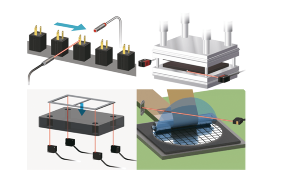
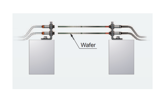
Wafer inclination detection can be valuable in several equipment modules where orientation stability influences downstream process performance, such as:
- Automated wafer handling systems (robot pick/place verification)
- Load port and transfer-related modules where wafer position deviations can escalate quickly
- Inspection-related handling steps where stable presentation supports consistent measurement conditions
Watch the video:
FAQ – Wafer inclination detection
|
Why is wafer inclination difficult to detect during transfer?
|
Wafer inclination is difficult to detect because it mainly occurs while the wafer is moving rather than when it is stationary. Most conventional sensors are designed to confirm presence only and do not provide information about alignment or angle. As a result, small deviations often go unnoticed until they cause mechanical contact or process variation further downstream.
|
|
What causes wafer tilt in semiconductor handling systems?
|
Wafer tilt is typically caused by small variations in the handling process, such as slight misalignment during pick-and-place, tolerances in robot mechanics, or positioning differences inside carriers like FOUPs. These effects occur dynamically during movement, which makes them difficult to identify without continuous measurement.
|
|
How can laser sensors detect wafer inclination in motion?
|
Laser-based sensors can detect wafer inclination by continuously measuring the position of the wafer while it is being transferred. Instead of only confirming presence, they provide precise distance data that reveals even small angular deviations. This allows inclination to be detected in real time before the wafer reaches the next process step.
|
|
Why is early detection critical to prevent wafer damage?
|
Early detection is critical because even small wafer inclinations can lead to mechanical contact with tool components or instability in subsequent processes. Once a tilted wafer enters a sensitive module, the risk of breakage or yield impact increases significantly. Detecting this during transfer allows immediate correction or rejection, reducing damage and improving overall system stability.
|
|
What is the impact of wafer inclination on process stability?
|
Wafer inclination can introduce variation in positioning, which affects how the wafer interacts with equipment in subsequent steps. This can lead to inconsistent processing conditions, increased defect risk and reduced yield. Maintaining correct wafer alignment is therefore essential for stable and repeatable semiconductor processes.
|