
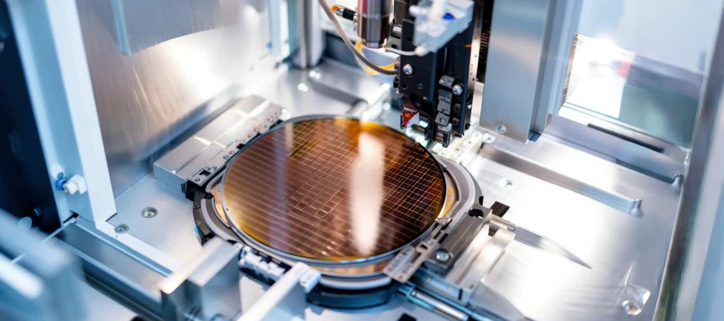
Semiconductor front-end resist stripping process
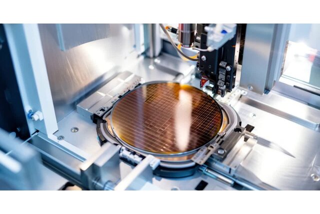
After etching, the remaining photoresist layer must be completely removed to prepare the wafer for the next process steps. This stage is critical to restore a clean and stable surface, ensuring that subsequent processing can take place under controlled conditions.
Resist stripping typically combines plasma-based ashing and wet chemical cleaning to remove both bulk resist and fine residues. At nanometer scale, incomplete removal or unstable process conditions can lead to contamination, defects or performance variation.
For semiconductor equipment builders, resist stripping is therefore not only a cleaning step, but a key process to reset surface conditions and ensure process continuity.
What challenges define the resist stripping process?
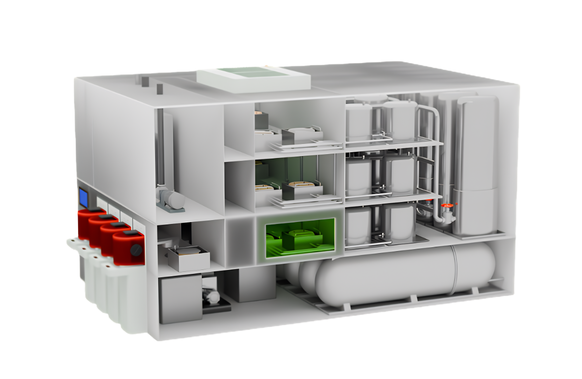
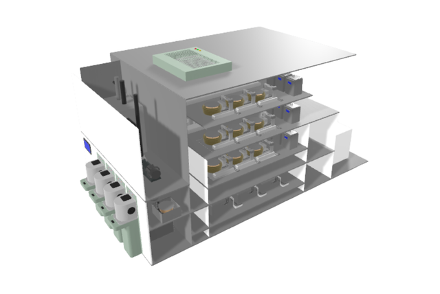
Resist stripping operates in demanding environments, combining plasma reactions, chemical cleaning and precise chamber control. Maintaining stability throughout this process is complex.
The wafer surface must be cleaned thoroughly without damage, while process parameters such as pressure, temperature and plasma conditions must remain stable. At the same time, detection and monitoring need to operate reliably without influencing the process.
Even small deviations, such as incomplete residue removal or unstable chamber conditions, can affect the quality of subsequent layers and reduce overall yield.
Plasma ashing and chemical cleaning
Ensuring complete resist removal
The stripping process typically starts with plasma ashing, where oxygen plasma oxidizes and removes the photoresist. This is followed by wet cleaning steps to remove remaining residues.
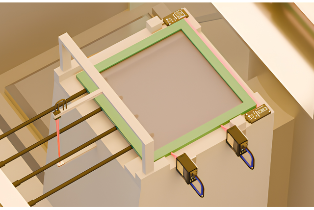
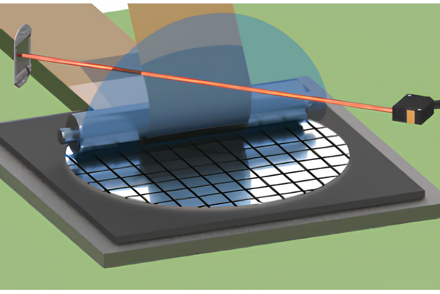
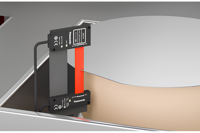
For this process to be effective, conditions must remain stable throughout the chamber. Panasonic Industry supports this with fiber optic sensing solutions (FT series with remote amplifiers) and photoelectric sensors, enabling reliable detection of wafer presence and process states without interfering with plasma conditions.
This ensures that every wafer is processed under controlled and repeatable conditions, resulting in consistent resist removal.
Detection and monitoring inside stripping systems
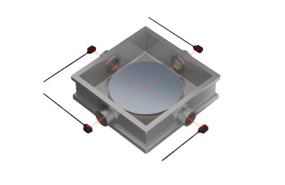
Maintaining process control in enclosed environments
Stripping systems operate as enclosed chambers where pressure and process conditions must be carefully controlled. Monitoring these parameters is essential to ensure consistent performance.
Panasonic Industry enables stable monitoring with compact laser sensors (EX‑L200 series) and fiber optic solutions, allowing detection within confined environments without adding heat or electrical interference.
By maintaining reliable feedback during the process, deviations can be detected early and corrected before they impact wafer quality.
Pressure and process condition monitoring
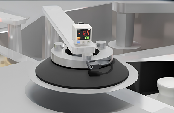
Ensuring stable plasma and cleaning conditions
Stable chamber pressure and process control are critical during both plasma and wet cleaning stages. Variations can lead to incomplete resist removal or surface damage.
Panasonic Industry provides pressure sensing solutions that continuously monitor chamber conditions, ensuring that process parameters remain within defined limits.
This allows the stripping process to operate consistently across wafers and over time.
Safety and leak detection
Protecting process stability and equipment
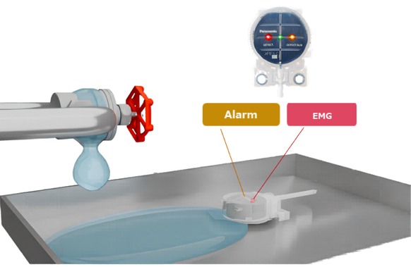
Chemical cleaning steps introduce additional risks related to leakage and contamination. Even small leaks can disrupt the process or damage equipment.
Panasonic Industry supports this with SQ4 leakage sensors, which provide early detection and enable rapid response before issues escalate.
By integrating safety monitoring into the system, downtime is reduced and process reliability is improved.
Why complete resist removal defines downstream performance
Resist stripping ensures that no residues remain on the wafer surface before the next process cycle begins. Any remaining contamination can affect adhesion, layer quality or electrical behavior in subsequent steps.
Because these effects are often subtle and only become visible later, this step plays a crucial role in maintaining overall process integrity.
Stable and complete resist removal ensures that the wafer is fully prepared for the next build-up cycle, supporting consistent device performance.
Panasonic Industry solutions for resist stripping processes
Panasonic Industry supports semiconductor equipment builders with sensing and control solutions designed for plasma and chemical environments.
These include:
- fiber optic sensing for non-intrusive detection
- photoelectric sensors for wafer presence
- laser sensors for monitoring in confined spaces
- pressure sensors for process control
- leakage detection for safety and reliability
Together, these technologies enable resist stripping processes that are stable, repeatable and ready for high-volume manufacturing.

FAQ – Resist Stripping
|
Why is resist stripping critical in semiconductor manufacturing?
|
Resist stripping is critical because it ensures that all photoresist and residues are removed before the next process step. Any contamination left on the wafer can affect layer quality, adhesion and overall device performance.
|
|
What makes resist stripping challenging?
|
The process combines plasma and chemical cleaning under tightly controlled conditions. Maintaining complete removal without damaging the wafer surface requires stable control of pressure, temperature and process parameters.
|
|
How does incomplete resist removal affect the process?
|
Incomplete removal can lead to contamination, affecting subsequent deposition or lithography steps. These issues often only become visible later, making them difficult to trace back to their origin.
|
|
Why is non-intrusive sensing important in stripping systems?
|
Sensors must operate without interfering with plasma or chemical reactions. Non-intrusive sensing ensures accurate monitoring while preserving stable process conditions.
|
|
How do leak detection and monitoring improve reliability?
|
Leak detection ensures that chemical processes remain controlled and safe. By identifying issues early, it prevents contamination, reduces downtime and maintains stable operation.
|