
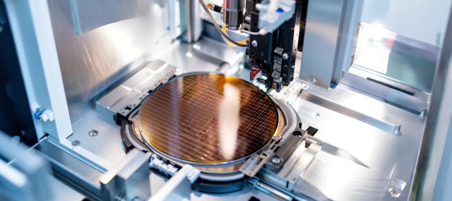
Semiconductor front-end film deposition process
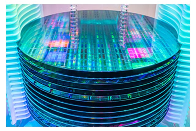
In semiconductor front-end manufacturing, the deposition process is used to apply ultra‑thin layers such as silicon oxide, silicon nitride or metal films onto the wafer surface. These layers form the foundation for device structures and directly influence electrical performance.
At nanometer scale, even small variations in temperature, wafer positioning or process conditions can affect:
- layer thickness uniformity
- film quality and adhesion
- long-term device reliability
Film deposition is therefore not only about forming layers, but about maintaining stable, repeatable process conditions across every wafer.
What challenges define the film deposition process?
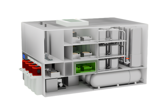
Deposition processes operate in highly controlled but demanding environments. Furnaces are used for oxidation, diffusion and annealing at high temperatures, while CVD and PVD systems deposit thin films under vacuum conditions.
Within these systems, maintaining stability is challenging. Wafers must be transported and positioned precisely, while process conditions such as temperature, vacuum and cleanliness must remain tightly controlled. Detection and monitoring need to function reliably without influencing the process itself.
At the same time, risks such as particle contamination, leakage or wafer misalignment can introduce variation that becomes visible only in later process steps.
The sections below explain how these challenges are addressed.
Wafer transport and positioning
Ensuring uniform layer deposition
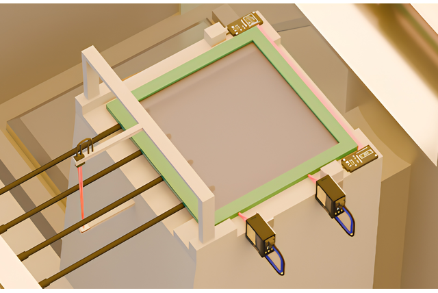
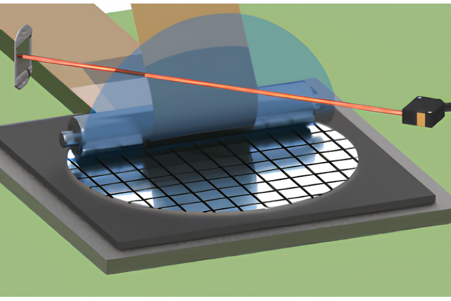
During film deposition, wafers must be transported and positioned with high precision to ensure uniform exposure to process conditions such as temperature and gas flow. Even small deviations can lead to variations in film thickness or material properties across the wafer.
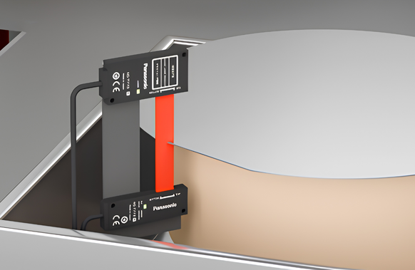
Panasonic Industry supports this critical step with laser and displacement sensing technologies such as the HG‑T transmission-type sensors and HG‑C / HL‑G series laser displacement sensors. These solutions provide accurate positioning feedback and allow equipment builders to verify wafer alignment during loading, positioning and processing.
By continuously monitoring wafer position, these sensors help maintain stable processing conditions, resulting in more uniform film growth and improved repeatability across wafers.
Detection in thermal and vacuum environments
Monitoring without influencing the process
Film deposition processes often take place under extreme conditions, including high temperatures in furnace systems and vacuum environments in CVD and PVD tools. In these environments, conventional sensors can introduce unwanted heat, contamination or electrical interference.
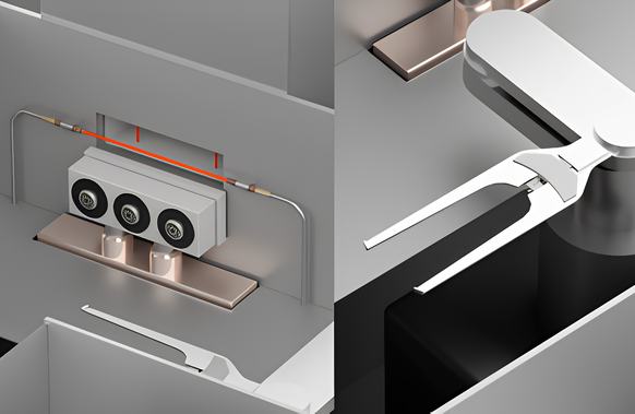
To address this, Panasonic Industry provides fiber optic sensing solutions (FT series) combined with remote amplifiers (FX / IO‑Link amplifiers). By separating the sensing head from the electronics, these solutions enable reliable detection inside the process environment without disturbing it.
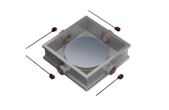
In addition, compact laser sensors such as the EX‑L200 series allow precise detection from outside the chamber or through protective interfaces. Together, these technologies enable stable and non-intrusive monitoring, even under highly constrained process conditions.
Wafer handling and mapping
Preventing variation during transfer
Before and after deposition, wafers are transferred between modules using robotic systems. Incorrect wafer seating, protrusion or mapping errors can introduce variation even before the deposition process begins.
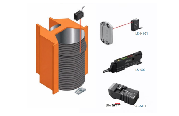
Panasonic Industry addresses this with a combination of fiber optic sensors (FT series) for wafer presence detection and laser-based sensing solutions such as LS‑500 or EX‑L200 for precise positioning and mapping. These sensors enable accurate detection of wafer position on robot blades and transfer stages.
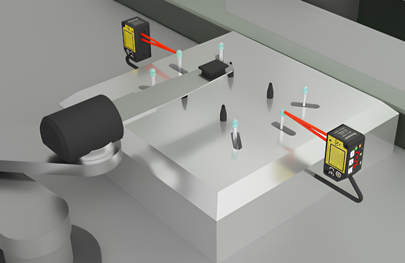
Additionally, displacement sensors such as HG‑C can detect wafer tilt or protrusion during transfer, allowing early correction before the wafer enters the process chamber.
By ensuring correct wafer handling and mapping, these solutions help maintain consistent starting conditions for deposition, reducing variability in downstream processes.
Safety and leak monitoring
Protecting process stability and equipment
Film deposition systems rely on controlled gases, vacuum integrity and chemical processes. Any leakage or instability can compromise both equipment performance and safety.
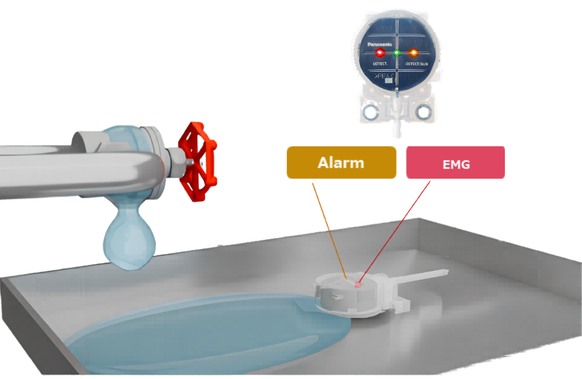
Panasonic Industry provides SQ4 safety leakage sensors, which enable reliable detection of liquid or chemical leakage with a two-stage output for early warning and emergency stop. This allows issues to be addressed before they lead to downtime or contamination.
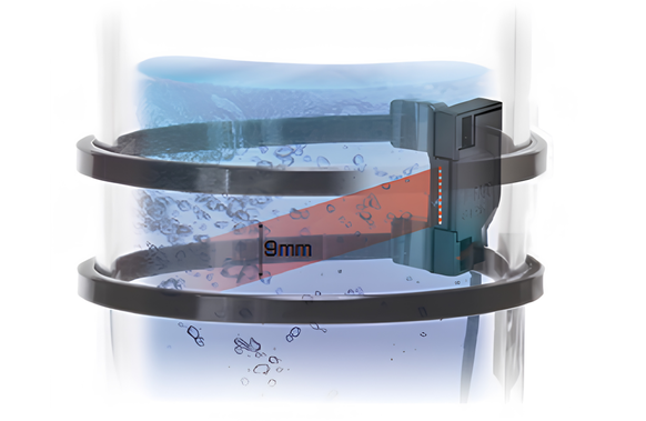
For monitoring process conditions, liquid level sensors such as EX‑F1 ensure stable detection of fluids without being affected by bubbles or residues. These sensors support consistent process control while maintaining safe operation.
Together, these solutions help minimize risk, protect equipment and ensure stable deposition conditions.
Electrostatic and contamination control
Maintaining clean and predictable process conditions
In deposition environments, electrostatic charge can influence particle movement and wafer behaviour. This increases the risk of contamination, which directly impacts film quality and device performance.
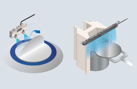
Panasonic Industry supports electrostatic control with ionizers such as the ER‑X and ER‑V series, which actively neutralize charge during wafer handling and processing. By reducing electrostatic effects, these solutions help prevent particle attraction and improve process cleanliness.
Combined with fiber optic sensing for non-intrusive detection, this approach ensures that monitoring and control do not introduce additional disturbances into the environment.
The result is a cleaner, more stable process that supports consistent film deposition and higher yield.
From wafer detection and chamber monitoring to machine control and operator visualization, Panasonic Industry combines sensing, PLC and HMI technologies to help semiconductor equipment manufacturers improve process stability, uptime and integration efficiency.
Machine control and process automation for semiconductor deposition equipment
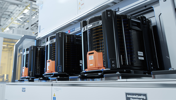
Ensure stable deposition processes through integrated machine control
Deposition equipment relies on precise coordination between wafer handling, chamber control, gas delivery, vacuum systems and safety interlocks. Maintaining process stability requires reliable control architectures that can continuously monitor and respond to changing process conditions.
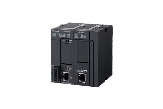
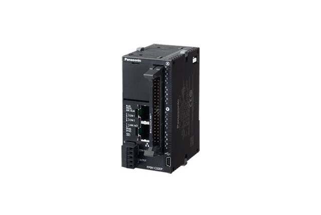
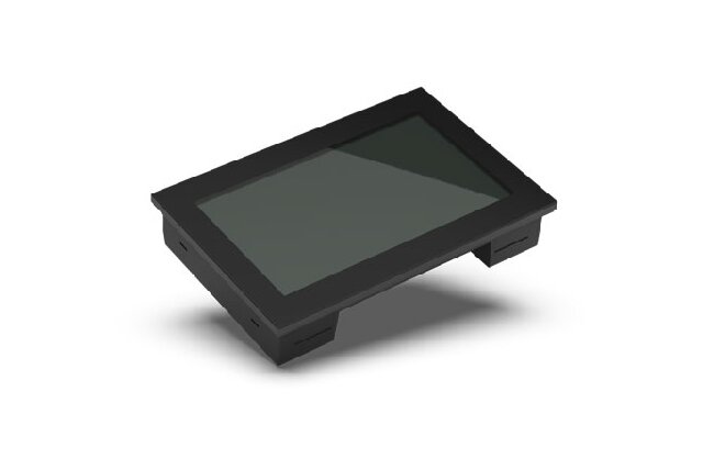
Panasonic Industry supports semiconductor equipment manufacturers with scalable PLC and HMI solutions that enable centralized machine control, process visualization and system diagnostics.
By integrating machine control and operator interfaces into deposition equipment, manufacturers can improve repeatability, reduce engineering complexity and support long-term equipment reliability.
Process data acquisition and traceability
Transform process data into actionable insights
Modern deposition systems generate large volumes of operational data from wafer positioning, pressure monitoring, liquid handling and environmental control systems.
Capturing and visualizing this information helps process engineers identify deviations earlier, improve chamber utilization and support traceability requirements throughout the semiconductor manufacturing lifecycle.
Panasonic PLCs and HMIs can collect and consolidate data from connected devices, enabling operators and maintenance teams to monitor process conditions in real time.
Benefits
- Improved process transparency
- Faster root-cause analysis
- Enhanced production traceability
- Real-time visualization of equipment status
- Simplified reporting and maintenance diagnostics
Why stability in deposition defines downstream performance
The quality of deposited films directly influences all subsequent process steps. Variations introduced during deposition can lead to:
- inconsistent etching behaviour
- deviations in electrical properties
- reduced overall yield
Because these effects are often difficult to correct later, deposition becomes a critical step in ensuring overall process stability.
Maintaining control at this stage helps ensure that downstream processes can perform as intended.
Panasonic Industry solutions for film deposition processes
Panasonic Industry supports semiconductor equipment builders with sensing, control and visualization technologies designed for thermal, vacuum and chemically controlled environments.
These include:
- compact sensing solutions for confined spaces
- fiber optic sensors for non-intrusive detection
- laser and displacement sensors for accurate positioning
- leakage detection and safety monitoring systems
- PLC-based machine control for process automation and data acquisition
- HMI solutions for process visualization, diagnostics and operator guidance
Together, these technologies enable equipment builders to create systems that are stable, scalable and reliable, supporting both development and high-volume manufacturing. By combining sensing, machine control and operator interfaces within a single automation architecture, OEMs can improve process consistency, equipment uptime and integration efficiency throughout the equipment lifecycle.
FAQ – Film Deposition Process
|
Why is film deposition critical in semiconductor manufacturing? |
Film deposition is critical because it defines the physical and electrical properties of semiconductor devices. The quality, thickness and uniformity of deposited layers directly influence how the device performs in later stages. Any variation introduced during deposition can affect downstream processes such as etching and patterning, making stability in this step essential. |
|
What makes film deposition processes challenging? |
Film deposition processes operate under controlled but demanding conditions such as high temperatures or vacuum environments. Within these conditions, wafers must be transported and positioned precisely, while sensors must operate without disturbing the process. Maintaining stability across all these factors is complex and requires carefully integrated sensing and control solutions. |
|
How can wafer positioning influence film quality? |
Wafer positioning plays a key role in ensuring uniform exposure to process conditions such as temperature and gas flow. If a wafer is slightly misaligned, it can lead to uneven layer thickness or variations in material properties. By continuously verifying wafer position, these deviations can be minimized and consistent film growth can be achieved. |
|
Why is non-intrusive sensing important in deposition systems? |
In deposition environments, even small disturbances can affect the process. Sensors that generate heat, light or electrical interference may influence film quality or introduce contamination. Non-intrusive sensing, such as fiber optic solutions, allows detection without affecting the environment, ensuring stable and reliable process conditions. |
| How do leak detection and monitoring contribute to process stability? |
Deposition systems rely on controlled gasses and vacuum conditions. Any leakage or instability can quickly disrupt the process or cause contamination. Early detection through dedicated sensing solutions allows operators to intervene before issues lead to downtime or yield loss, ensuring both safety and process reliability. |
|
How does film deposition impact downstream processes? |
The outcome of the deposition step directly affects subsequent processes such as etching and pattern transfer. Variations in deposited layers can lead to inconsistencies in later stages, which are often difficult to correct. Stable deposition therefore ensures that all following steps can perform under predictable and controlled conditions. |