
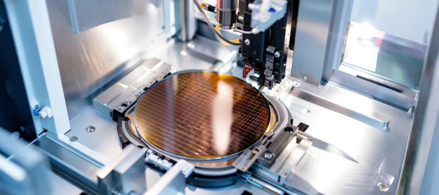
Semiconductor front-end Ion Implantation process
In semiconductor front-end manufacturing, ion implantation is used to modify the electrical properties of the wafer by embedding charged particles at controlled depth. This step defines critical characteristics such as conductivity and device behaviour at nanometer scale.
Because implantation relies on high-energy ion beams and precise positioning, even small deviations in beam alignment or wafer positioning can directly impact:
- dopant distribution
- electrical performance
- device uniformity
Ion implantation is therefore not only about introducing ions, but about maintaining stable and precisely controlled process conditions throughout the system.
What challenges define the ion implantation process?
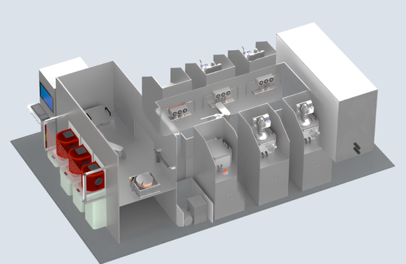
Ion implantation takes place in highly controlled environments, combining high voltages, vacuum conditions and magnetic field control to guide accelerated ions toward the wafer.
Within this setup, maintaining stability is complex. Ion beams must remain precisely aligned, wafer positioning must be accurate, and process conditions such as vacuum pressure and cooling must stay within tight limits. At the same time, detection and monitoring must function without introducing interference.
Even small disturbances in beam stability, alignment or system conditions can lead to variation that directly affects device performance. This makes reliable sensing and control essential throughout the implantation process.
Beam positioning and alignment
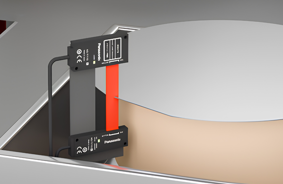
Ensuring accurate ion placement.
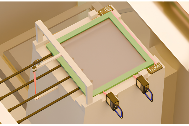
The accuracy of ion implantation depends on precise control of the ion beam. Any deviation in beam position or alignment can result in incorrect dopant placement, affecting device functionality.
Panasonic Industry supports this process with high-precision sensing solutions such as HG‑T digital displacement sensors and HL‑G / HG‑C laser displacement sensors, which enable precise positioning and alignment verification within the system.
By continuously monitoring beam-related positioning and mechanical alignment, these solutions help maintain stable implantation conditions and ensure consistent electrical characteristics.
Wafer presence and positioning
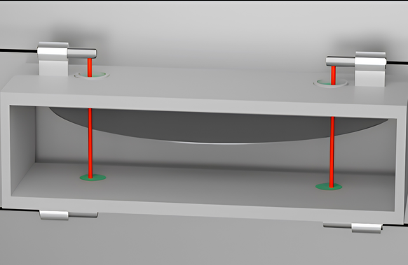
Maintaining stable interaction between beam and wafer.
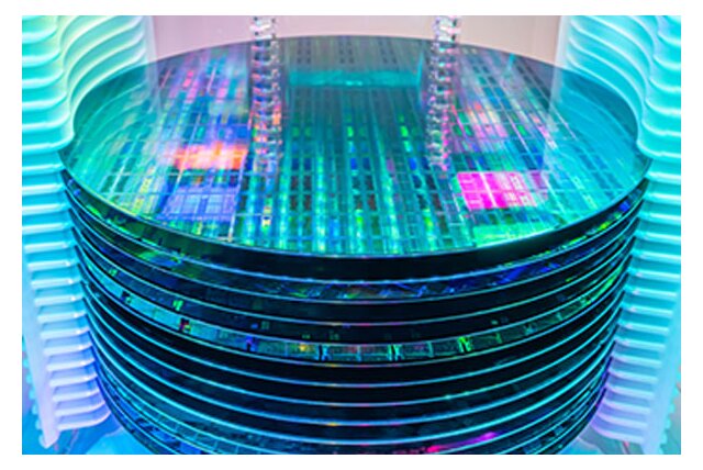
During implantation, wafers must be positioned accurately relative to the ion beam. Incorrect wafer placement or movement can lead to non-uniform implantation and variability across the wafer.
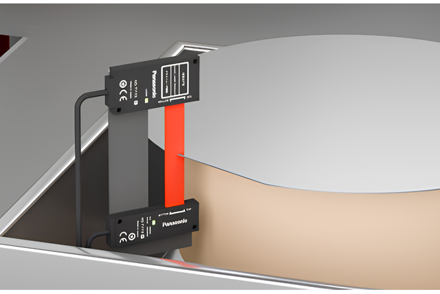
Panasonic Industry addresses this with photoelectric sensors and fiber optic sensing solutions (FX amplifiers with FT fiber heads), which enable reliable wafer detection even in confined or vacuum environments.
These technologies allow verification of wafer presence and positioning without disturbing the process, ensuring that each wafer is correctly aligned before and during implantation.
Detection in vacuum and high-energy environments
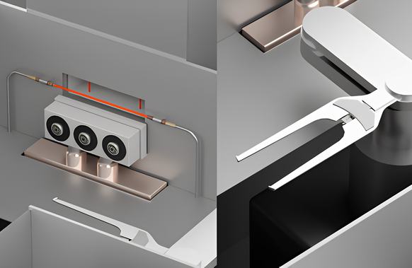
Monitoring without interference.
Ion implantation systems operate under deep vacuum and high-energy conditions, where conventional sensors may not be suitable.
To overcome this, Panasonic Industry provides fiber optic sensing solutions that separate the sensing head from electronics, allowing detection inside the chamber without introducing heat or electrical interference.
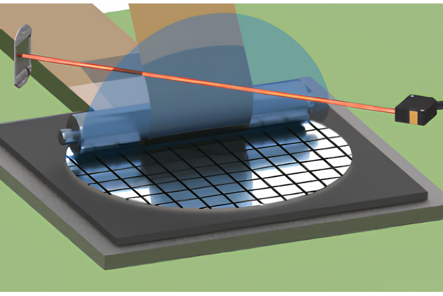
In addition, compact laser sensors (EX‑L200 series) enable detection from outside critical zones, supporting accurate monitoring without affecting beam behaviour or process stability.
Pressure, flow and cooling control
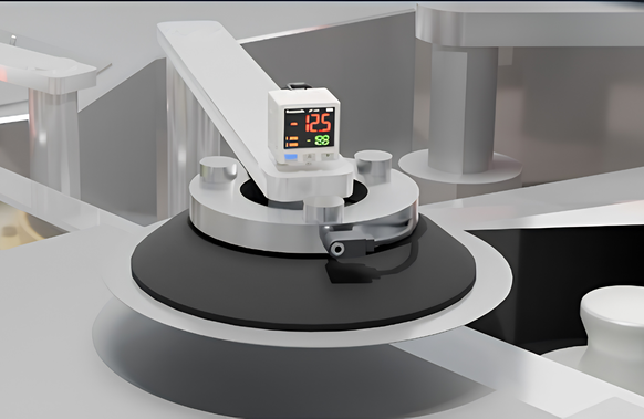
Keeping process conditions stable.
Implantation systems rely on stable vacuum conditions and controlled cooling to maintain process integrity. Variations in pressure or cooling flow can impact beam stability and overall system performance.
Panasonic Industry supports this with pressure and flow sensing solutions, enabling continuous monitoring of critical parameters within the chamber and cooling systems.
By detecting deviations early, these solutions help maintain stable operating conditions and prevent process disruptions.
Safety and process monitoring
Protecting system performance and reliability.
Given the high-energy nature of ion implantation, safety and system monitoring are critical. Early detection of anomalies ensures both equipment protection and process continuity.
Panasonic Industry solutions enable continuous monitoring of system conditions, allowing deviations to be identified before they lead to downtime or performance loss.
This ensures that the implantation process remains stable, controlled and reliable.
Why stability in ion implantation defines device performance
Ion implantation defines key electrical properties of semiconductor devices. Any variation introduced at this stage directly affects how devices function.
Unlike some other steps, implantation errors cannot easily be corrected later in the process flow. Variability in dopant placement can lead to:
- inconsistent electrical behaviour
- reduced device performance
- yield loss
This makes implantation a critical control point where precision and stability must be guaranteed.
Panasonic Industry solutions for ion implantation processes
Panasonic Industry supports semiconductor equipment builders with sensing and control technologies designed for high-energy, vacuum-based environments.
These include:
- laser and displacement sensors for alignment and positioning
- fiber optic sensing for non-intrusive detection
- photoelectric sensors for wafer detection
- pressure and flow sensors for vacuum and cooling control
Together, these technologies enable stable, repeatable and scalable ion implantation processes.
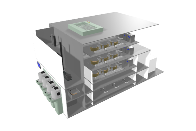
FAQ – Ion Implantation
|
What makes ion implantation processes challenging? |
Ion implantation combines high-energy beams, vacuum conditions and precise positioning requirements. Maintaining stable beam alignment and consistent process conditions under these circumstances is complex and requires advanced sensing and control. |
| How does beam alignment affect implantation results? |
Beam alignment determines where ions are embedded in the wafer. Even small deviations can lead to incorrect dopant distribution, affecting electrical performance and device consistency. |
|
Why is non-intrusive sensing important in ion implantation systems? |
In high-energy and vacuum environments, sensors must not interfere with the process. Non-intrusive sensing ensures accurate monitoring without affecting beam behaviour or process conditions. |
|
How do pressure and flow control influence process stability? |
Stable vacuum and cooling conditions are essential to maintain beam stability and system performance. Variations in pressure or flow can introduce process instability and affect implantation accuracy. |