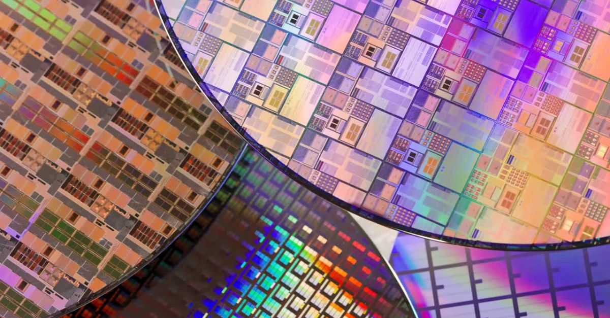
Metrology starts with stable CMP chemistry delivery
Stable CMP chemistry delivery is essential for reliable semiconductor metrology. In semiconductor manufacturing, metrology tools translate physical variations into process data. That data is only meaningful when the upstream process conditions are stable.
For CMP processes, this means chemistry delivery must be consistent wafer after wafer. Even small disturbances in flow can introduce variation that metrology tools will detect, but cannot correct.
As device geometries shrink and process windows tighten, metrology reliability increasingly depends on process stability before measurement.
The CMP chemistry challenge: identical dosing on every wafer
The goal of CMP chemistry delivery sounds straightforward:
- every wafer receives the same amount of chemistry,
- delivered in a stable and repeatable way.
In reality, two common disturbances frequently introduce variability:
- Air bubbles that interrupt the continuity of the flow
- Small clumps or aggregates that locally change flow behavior
Even short bubble events can cause wafer‑to‑wafer variation. From a metrology perspective, this shows up as noise, drift, or false excursions, signals that should never reach the data analysis stage.
Why metrology tools are affected first
Metrology systems are designed to detect tiny deviations. When chemistry delivery fluctuates, metrology tools will:
- identify variation that is not caused by the process recipe,
- trigger investigations into issues that originate upstream,
- consume engineering time resolving “measurement problems” that are actually supply‑line issues.
For tool builders and fabs, this creates unnecessary complexity and downtime.
A practical mitigation strategy: detect bubbles before dispensing
One effective and equipment‑friendly approach is inline bubble detection, installed before the final dispense point.
By detecting air gaps in the chemistry supply line early, variability can be prevented from reaching the wafer, reducing the burden on metrology and process control systems.
Optical bubble sensing is especially suitable for CMP applications because it:
- does not obstruct flow,
- works with small‑diameter tubing,
- reacts fast enough to detect short bubble events.
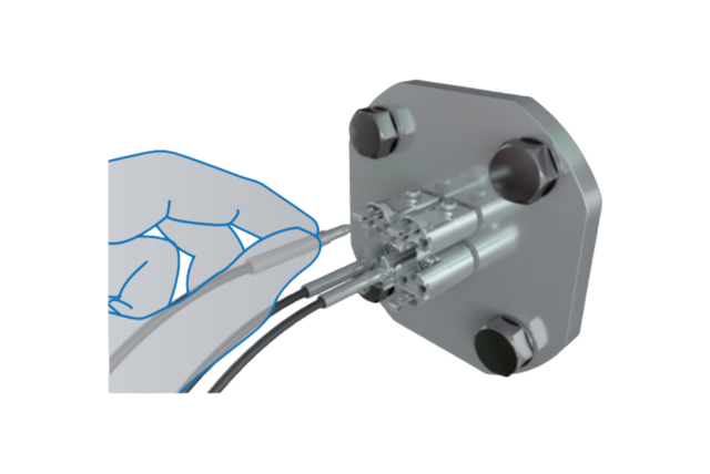
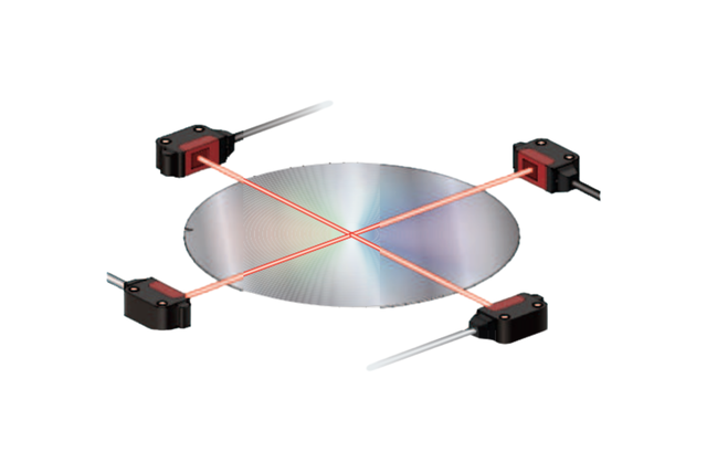
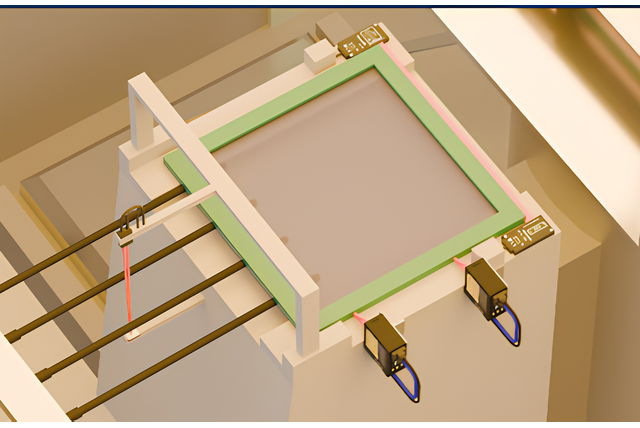
Optical bubble sensing for CMP: application overview
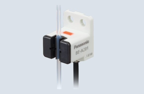
Optical bubble sensors are mounted directly around transparent tubing and detect changes in light transmission caused by air gaps in the liquid.
For CMP chemistry delivery, typical integration points include:
- upstream of the final dispense nozzle,
- after valves or switching points,
- after filtration or conditioning stages.
Placing the sensor close to the dispence point ensures that disturbances are detected before they affect the wafer.
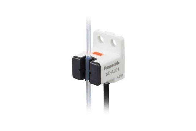
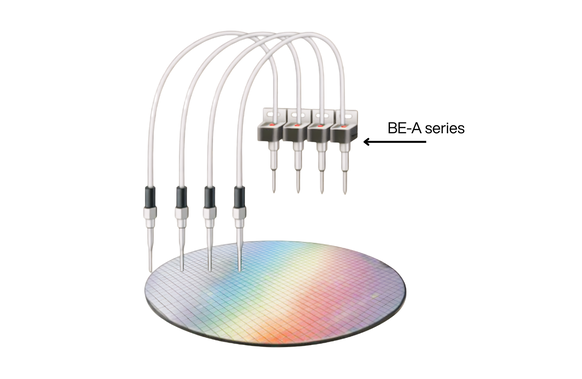
Solution example: Panasonic BE A series bubble sensors
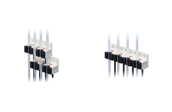
Panasonic Industry’s optical bubble sensors are designed for small‑diameter tubing commonly used in semiconductor equipment.
BE‑A201P for standard CMP lines
For 2 mm PFA‑equivalent tubing, the BE‑A201P is a typical choice:
- detects air gaps ≥ 0.8 mm,
- response time in the microsecond range,
- compact form factor,
- no contact with the liquid,
- simple mechanical installation.
BE‑A301P for custom tubing
For applications using 3 mm tubing, the same BE‑A family includes a 3 mm variant.
This allows equipment designers to maintain a consistent sensing concept across different fluid line dimensions.
Optical bubble sensors detect air gaps above a specified threshold. Very small micro‑bubbles or droplets may not be detected. Tube cleanliness and regular validation in the actual tool environment remain part of good engineering practice.
What metrology tool builders gain in practice
Adding bubble detection to CMP chemistry delivery supports several key objectives:
- More repeatable dosing
Less wafer‑to‑wafer variation caused by supply instability. - Cleaner metrology signals
Reduced noise and fewer false process excursions. - Higher tool uptime
Fewer investigations into issues that originate outside the metrology system. - Faster root‑cause analysis
Disturbances are detected at the source, not after the wafer is processed.
These gains directly support the semiconductor industry’s demand for reliability and consistency at nanometer scale.