
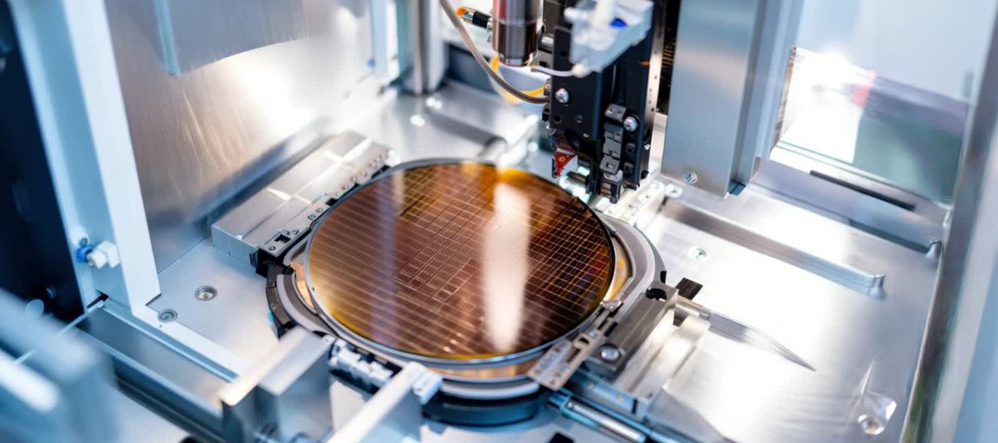
Semiconductor back-end wafer dicing process
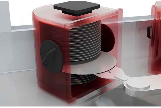
In semiconductor back-end manufacturing, wafer dicing separates processed wafers into individual dies. This step is critical for preparing chips for packaging and assembly.
Dicing is typically performed using high-speed mechanical saws or laser-based systems, where precision and stability are essential. At this stage, wafers are already thinned and highly sensitive, meaning even small instabilities can lead to:
- chipping or cracking
- particle contamination
- die damage or yield loss
Wafer dicing is therefore not only about cutting, it is about ensuring stable wafer handling, controlled process conditions and clean separation throughout the entire operation.
What challenges define the dicing process?
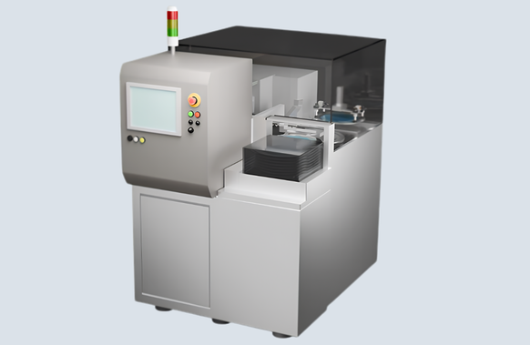
Wafer dicing combines high-speed mechanical cutting with precise wafer handling and continuous cooling. The wafer must remain stable during cutting, while debris and particles must be removed effectively.
At the same time, multiple subsystems must operate in coordination:
- wafer mounting and fixation
- blade condition and positioning
- cooling water flow
- contamination control
- transfer and handling before and after cutting
Even small deviations, such as wafer protrusion, insufficient suction or unstable cooling, can directly result in damage or reduced yield.
Wafer fixation and suction control
Ensuring stability during cutting
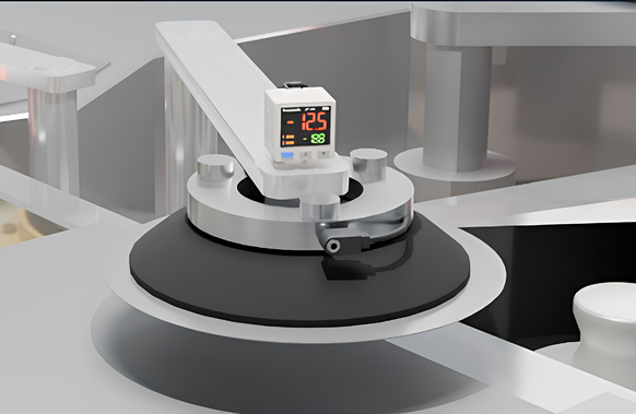
During dicing, wafers are mounted and fixed on a chuck or tape. Stable suction is essential to prevent movement during high-speed cutting operations.
Panasonic Industry supports this with digital pressure sensors such as the DPH‑100 / DPS‑400 series, enabling fast and accurate verification of wafer adsorption.
These sensors detect vacuum conditions in real time, ensuring that wafers remain securely fixed before and during cutting. This reduces the risk of movement and improves cutting accuracy.
Wafer presence, protrusion and positioning
Preventing damage before cutting starts
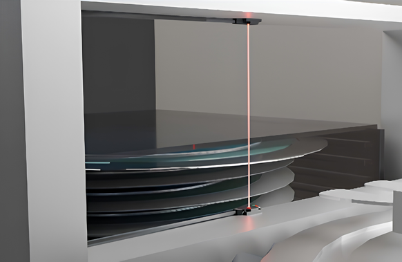
Before the cutting process begins, correct wafer positioning must be verified. Even a small protrusion or misalignment can lead to breakage or chipping during sawing.
Panasonic Industry provides compact photoelectric sensors (EX‑10 / EX‑19 series) to detect wafer protrusion and positioning with high precision.
In addition, fiber optic sensors (FD‑L13H1) enable highly accurate wafer seating detection within compact robot hands, ensuring correct alignment before processing.
These solutions allow early detection of misplacement, preventing damage before it occurs.
Blade condition and wear monitoring
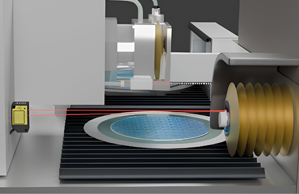
Maintaining consistent cutting performance
Cutting performance depends heavily on the condition of the dicing blade. As blades wear down over time, cutting accuracy and surface quality can degrade.
Panasonic Industry supports blade monitoring with laser displacement sensors such as the HG‑C and HL‑G2 series, which provide precise measurement of blade position and wear.
By monitoring blade condition continuously, equipment builders can maintain consistent cutting quality and reduce process drift.
Cooling and liquid monitoring
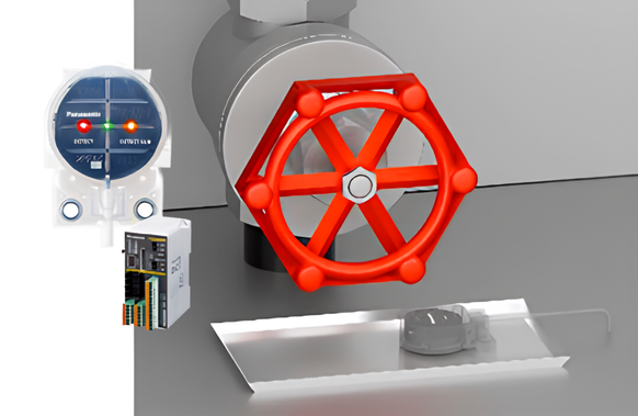
Dicing requires continuous cooling to manage heat and remove debris generated during cutting. Any disruption in cooling flow can affect cutting quality and damage the wafer.
Panasonic Industry provides:
- liquid level sensors (EX‑F / FD series) to monitor cooling flow
- leakage sensors such as the SQ4 series for early detection of fluid leaks
These solutions ensure that cooling conditions remain stable and prevent downtime caused by fluid-related issues.
Electrostatic control and contamination prevention
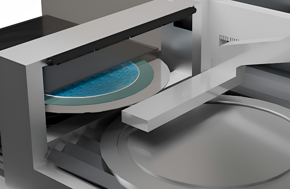
Maintaining clean die separation
During high-speed cutting and wafer transfer, electrostatic charge can build up, attracting particles and increasing contamination risk.
Panasonic Industry addresses this with ionizers such as the ER‑X and ER‑V series, which provide fast and controlled charge neutralisation.
By reducing electrostatic effects, these solutions help minimize particle adhesion and ensure cleaner die surfaces after cutting.
Motion and safety control
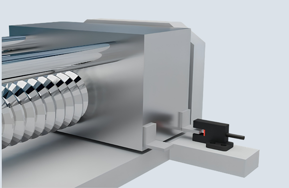
Ensuring reliable machine operation
Dicing systems contain multiple moving components that must operate safely and accurately. Reliable detection of movement and positioning is essential.
Panasonic Industry supports this with:
- photoelectric sensors (PM series) for position detection
- safety solutions such as SF‑C21 controllers for safe system integration
These technologies ensure that machine movement remains controlled and safe throughout operation.
Why stability in dicing defines yield and quality
Dicing is one of the final process steps before packaging. Any defect introduced at this stage directly affects the final product and cannot be corrected later.
Instabilities can lead to:
- die chipping or breakage
- contamination of die surfaces
- reduced packaging yield
This makes dicing a critical control point where process stability directly determines product quality.
Panasonic Industry solutions for dicing processes
Panasonic Industry supports semiconductor equipment builders with sensing and control solutions tailored for high-speed cutting environments.
These include:
- pressure sensors for wafer suction verification
- fiber sensors for wafer seating detection
- photoelectric sensors for positioning and protrusion detection
- ionizers for electrostatic control
- leakage sensors for cooling system stability
Together, these technologies enable dicing processes that are stable, precise and scalable for high-volume production.
FAQ – Wafer Dicing
|
Why is wafer dicing critical in semiconductor manufacturing? |
Wafer dicing separates the wafer into individual dies that will be packaged into final devices. Any defects introduced at this stage directly impact final product quality. |
|
What are the main challenges in wafer dicing? |
The main challenges include maintaining wafer stability during cutting, controlling blade wear, ensuring proper cooling and minimizing contamination. |
| How does wafer positioning affect dicing quality? |
Incorrect positioning or protrusion can cause mechanical stress during cutting, leading to wafer damage or incorrect cuts. |
|
Why is cooling important in dicing processes? |
Cooling prevents overheating and removes debris during cutting. Stable cooling conditions are essential for consistent cutting quality. |
|
How does electrostatic control improve dicing results? |
Reducing electrostatic charge minimizes particle attraction, resulting in cleaner die surfaces and improved yield. |