
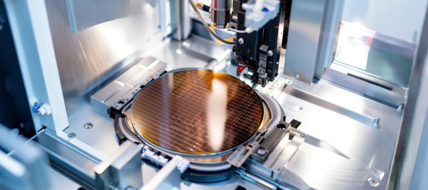
Semiconductor back-end test handling process
In semiconductor back-end manufacturing, test handling ensures that packaged devices are transported, positioned and routed correctly during electrical testing and binning.
This step connects manufacturing with final product qualification. Devices must be handled at high speed while maintaining precise positioning and stable contact conditions.
Even small instabilities in transfer, alignment or contamination control can lead to:
- contact failures during testing
- incorrect binning
- mechanical damage to devices
Test handling is therefore not only about moving devices, but about ensuring stable, precise and repeatable transfer throughout the entire test flow.
What challenges define the test handling process?
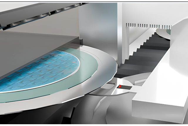
Test handling involves complex, high-speed movement of devices between trays, test sockets and sorting systems. Multiple variables must remain stable at the same time.
Devices must be correctly positioned for contact, while transfer systems must detect presence, orientation and placement continuously. At the same time, electrostatic effects and contamination must be controlled to avoid damaging sensitive devices.
Because test handling operates at high throughput, even small errors can propagate quickly and impact productivity.
Tray handling and device detection
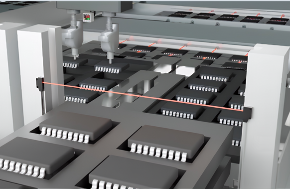
Ensuring accurate transfer into test contact
Devices are transported in trays or strips that must be positioned precisely before entering the test socket. Any misalignment or incorrect tray positioning can lead to contact issues.
Panasonic Industry supports this with ultra-compact photoelectric sensors (EX‑10 / EX‑13 / EX‑Z series), which enable reliable detection of tray presence and positioning even in space-constrained systems.
These sensors provide stable detection without complex setup, supporting fast and accurate transfer into test contact.
Device presence and seating verification
Preventing contact errors during testing
Before testing, each device must be correctly seated and positioned. Incorrect placement can result in unreliable electrical contact or device damage.
Panasonic Industry provides fiber optic sensing solutions (FX‑250 / FX‑500 amplifiers with FT fiber heads), which enable highly accurate detection of device presence and position, even within complex tray structures.
These solutions allow detection of small variations such as floating or misaligned ICs, preventing errors before testing begins.
Vacuum and suction monitoring
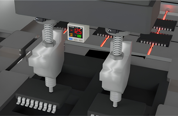
Ensuring stable device handling
Many test handling systems rely on vacuum-based pick-and-place systems. Stable suction is critical to ensure that devices are handled safely during transfer.
Panasonic Industry supports this with digital pressure sensors (DPH‑100 / DPS‑400 series), which provide fast and accurate monitoring of suction conditions.
By verifying vacuum conditions in real time, these sensors help prevent handling errors and ensure consistent device transfer.
Motion and position detection
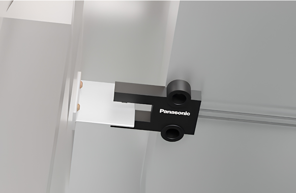
Controlling high-speed mechanical movement
Test handlers contain multiple moving components operating at high speed. Accurate detection of movement and position is essential for reliable operation.
Panasonic Industry offers:
- photoelectric sensors (PM series) for detecting moving components
- fiber-based fork sensors (FT‑PK series) for precise position detection in compact or high-temperature environments
These solutions ensure that each movement is controlled and verified, supporting stable system performance.
Electrostatic control and contamination prevention
Protecting sensitive devices during transfer
During high-speed transport, electrostatic charge can build up on devices and trays, increasing the risk of contamination or device damage.
Panasonic Industry addresses this with ionizers such as the ER‑F and ER‑X series, which provide controlled and fast neutralisation of static charge.
This reduces particle attraction and ensures clean handling conditions for sensitive semiconductor components.
Leak detection and safety monitoring
Ensuring system reliability and uptime
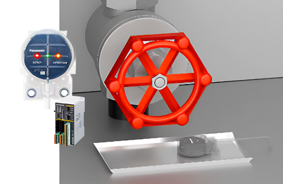
Cooling and environmental control systems are essential for stable handler operation. Leakage or system instability can disrupt testing and reduce throughput.
Panasonic Industry provides:
- leakage sensors such as the SQ4 series for early detection
- fiber-based leak sensors for compact installation
These solutions detect issues early, preventing downtime and ensuring safe and stable operation.
Binning and routing control
Ensuring correct sorting after testing
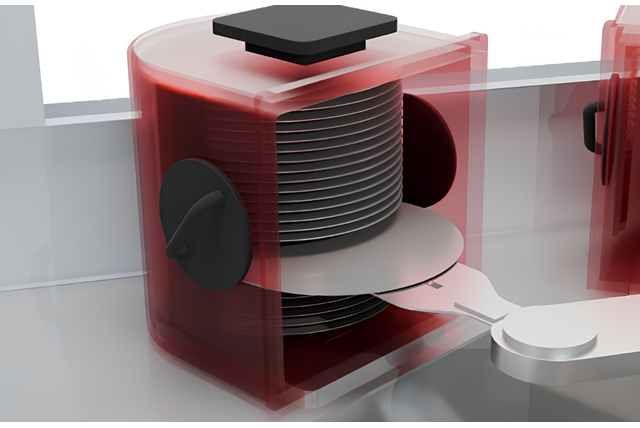
After testing, devices must be routed to the correct bin based on test results. Any misplacement can lead to quality issues or sorting errors.
Panasonic Industry sensing solutions enable accurate verification of device arrival and placement, ensuring that sorting remains stable and predictable throughout the system.
Why stability in test handling defines final product quality
Test handling is one of the final stages before shipment. Errors introduced here directly affect product quality and cannot be corrected afterward.
Instabilities can lead to:
- incorrect test results
- mis-sorted devices
- mechanical damage
This makes test handling a critical control point for ensuring consistent and reliable final output.
Panasonic Industry solutions for test handling processes
Panasonic Industry supports semiconductor equipment builders with sensing and control technologies designed for high-speed and high-precision environments.
These include:
- compact photoelectric sensors for tray and device detection
- fiber optic sensors for high-precision presence verification
- pressure sensors for vacuum control
- ionizers for electrostatic protection
- leakage sensors for system monitoring
Together, these technologies enable test handling systems that are stable, repeatable and optimized for high-throughput production.

FAQ – Test Handling
|
Why is test handling critical in semiconductor manufacturing? |
Test handling ensures that devices are correctly positioned and transported during electrical testing and sorting. Errors at this stage directly affect final product quality. |
|
What are the main challenges in test handling? |
Challenges include maintaining stable transfer, ensuring correct device positioning, controlling electrostatic charge and preventing misplacement during high-speed operation. |
|
How does device positioning affect test results? |
Incorrect positioning can lead to poor electrical contact, resulting in inaccurate test results or device damage. |
|
Why is vacuum monitoring important in test handling? |
Vacuum systems are used for picking and placing devices. Stable suction ensures reliable handling and prevents device drops or misplacement. |
|
How does electrostatic control improve reliability? |
Reducing electrostatic charge prevents particle attraction and protects sensitive devices during transfer and handling. |